
Processing method of surface periodic conical microstructure based on Gaussian beam focusing direct writing

A processing method, Gaussian beam technology, applied in the direction of metal processing equipment, manufacturing tools, laser welding equipment, etc., can solve the problems of low efficiency and slow processing speed, and achieve the effect of high efficiency, fast speed and simple process flow

Active Publication Date: 2021-02-12
TIANJIN JINHANG INST OF TECH PHYSICS
View PDF6 Cites 1 Cited by
  • Summary
  • Abstract
  • Description
  • Claims
  • Application Information

AI Technical Summary

Problems solved by technology

Although this method makes full use of the energy of the laser, it needs to process the non-planar three-dimensional structure multiple times, the processing speed is slow and the efficiency is low, and it cannot realize the non-planar structure surface processing with high continuity requirements, which is difficult to be efficient and fast. Realize the formation of fine three-dimensional structures on the surface of large-area optical materials

Method used


Image

  • Processing method of surface periodic conical microstructure based on Gaussian beam focusing direct writing
  • Processing method of surface periodic conical microstructure based on Gaussian beam focusing direct writing
  • Processing method of surface periodic conical microstructure based on Gaussian beam focusing direct writing

Examples


Embodiment

[0048] In this embodiment, the surface periodic conical microstructure processing method based on Gaussian beam focused direct writing is used to process the microstructure on the surface of the infrared substrate material ZnS. Write processing.

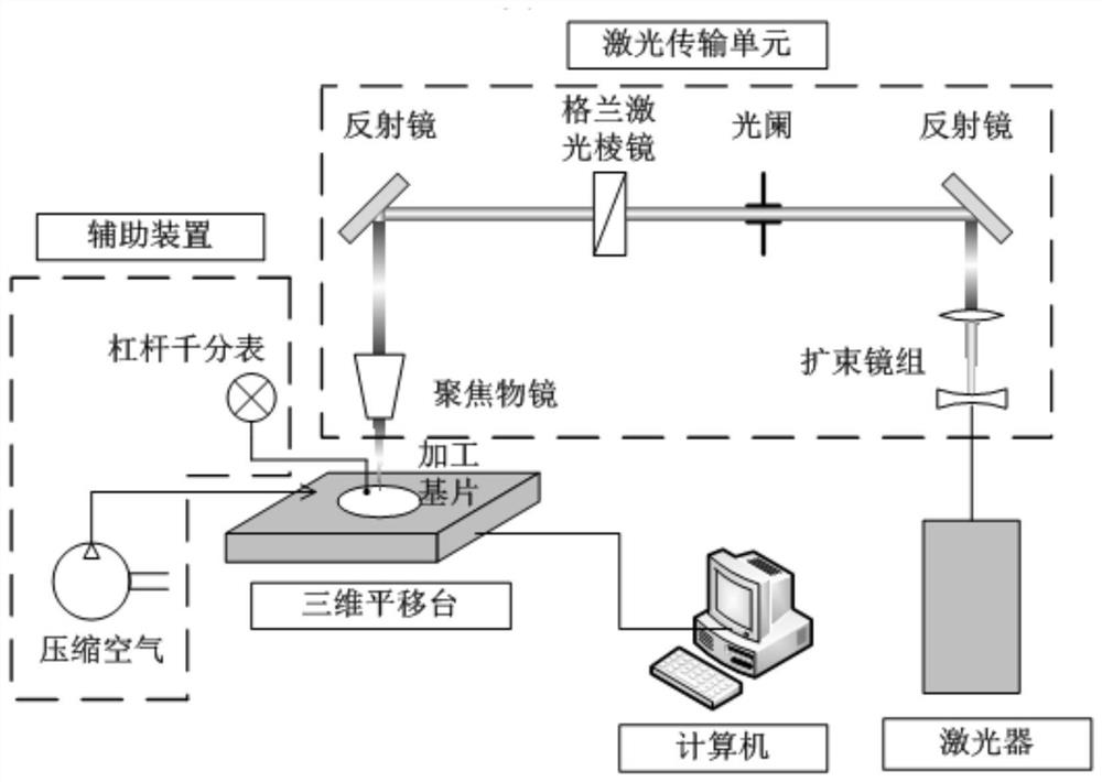
[0049] This embodiment adopts as figure 2 The Gaussian beam focusing direct writing system shown is realized. like figure 2 As shown, the system includes: a laser, a laser transmission unit, an auxiliary device, a three-dimensional translation platform and a computer.

[0050] like figure 2 As shown, the laser light source is a femtosecond laser with a pulse width of 40fm and a wavelength of 800nm; the laser transmission unit at least includes: a beam expander mirror group, a first reflector, an aperture, a Glan laser prism, a second reflector and a focusing objective lens . The Gaussian beam emitted by the laser light source passes through the above-mentioned optical path, and is focused and output to the three-dimensional t...


PUM


Abstract

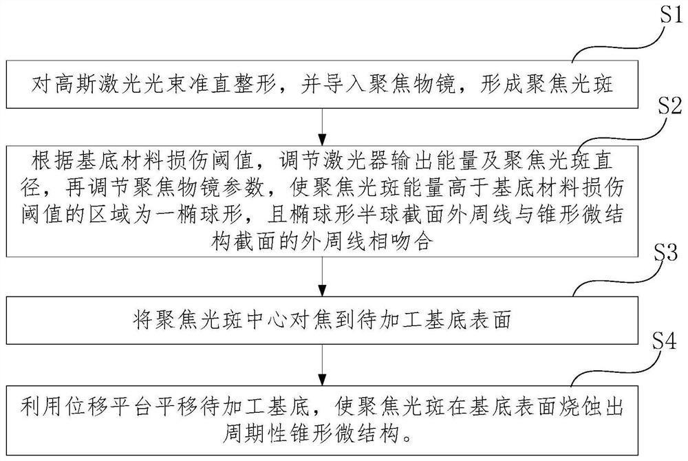
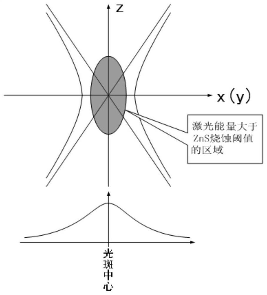
The invention provides a processing method of a surface periodic conical microstructure based on Gaussian beam focusing direct writing, and aims to solve the problem of low processing efficiency of alarge-area surface periodic conical microstructure in the prior art. The processing method of the surface periodic conical microstructure comprises the following steps of: firstly, importing a Gaussian laser beam into a focusing objective lens to form a light spot; then, adjusting relevant parameters according to a substrate material damage threshold value, so that an area, of which the focusing light spot energy is higher than the substrate material damage threshold value, is ellipsoidal; and after the light spot is focused to a substrate processing surface, translating a substrate to be processed by utilizing a displacement platform, so that the focusing light spot ablates the periodic conical microstructure on the surface of the substrate. According to the processing method, high-precision focusing is not needed, the conical periodic microstructure is directly formed on the surface of the substrate by utilizing the energy distribution gradient of the Gaussian beam after focusing andthrough a scanning motion form, and the processing of a fine three-dimensional structure is completed at one time, so that the speed is high, the efficiency is high, the process flow is simple, and high-precision continuous non-planar processing can be realized.

Description

technical field [0001] The invention belongs to the field of micro-nano processing, in particular to a method for processing surface periodic tapered microstructures based on Gaussian beam focused direct writing. Background technique [0002] The surface microstructure of optical materials can solve technical bottlenecks that cannot be solved by traditional optical films such as anti-reflection and depolarization at large angles of light incidence, broadband anti-reflection, and long-term hydrophobic surfaces. The microstructure is usually processed by means of laser etching or the like. [0003] In the prior art, when it is necessary to process a three-dimensional microstructure, the uniform spot of a laser is usually used to process structural surfaces with different depths and sizes on the surface to be processed in stages, thereby constructing a three-dimensional microstructure. Although this method makes full use of the energy of the laser, it needs to process the non-...

Claims


Application Information

Patent Timeline
Patent Type & Authority Applications(China)
IPC IPC(8): B23K26/362B23K26/064
CPCB23K26/362B23K26/064B23K26/0643B23K26/0652
Inventor 杨霄姜玉刚刘华松刘丹丹
Owner TIANJIN JINHANG INST OF TECH PHYSICS
Learn More