Design method for multi-wavelength ultrashort-pulse mode-locked photonic integrated chip with high repetition frequency, product and application

A technology of photon integration and ultrashort pulse, which is applied in the direction of optical waveguide light guide, optics, light guide, etc., can solve the problems that the mode-locked laser can only work independently, and the output frequency of the four channels is not completely consistent, so as to provide technical support and reduce the cost of devices. Cost, the effect of breaking the speed bottleneck

Active Publication Date: 2021-02-12
ZHEJIANG UNIV
View PDF4 Cites 4 Cited by
  • Summary
  • Abstract
  • Description
  • Claims
  • Application Information

AI Technical Summary

Problems solved by technology

In 2010, Lianping Hou et al. from the University of Glasgow used quantum well hybrid (QWI) technology to realize a four-wavelength semiconductor mode-locked laser for the first time, but the output frequencies of the four channels are not completely consistent.
Caltech previously reported an integrated chip consisting of nine parallel collision mode-locked lasers (CPM), which can only work independently

Method used


Image

  • Design method for multi-wavelength ultrashort-pulse mode-locked photonic integrated chip with high repetition frequency, product and application
  • Design method for multi-wavelength ultrashort-pulse mode-locked photonic integrated chip with high repetition frequency, product and application

Examples


Embodiment Construction

[0025] In order to make the object, technical solution and advantages of the present invention clearer, the present invention will be further described in detail below in conjunction with the accompanying drawings and embodiments. It should be understood that the specific embodiments described here are only used to explain the present invention, and do not limit the protection scope of the present invention.

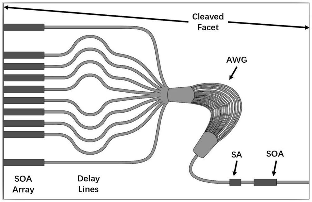
[0026] figure 1 A schematic structural diagram of a mode-locked photonic integrated chip with high repetition rate and multi-wavelength ultrashort pulses provided by an embodiment of the present invention. like figure 1 As shown, the high-repetition-frequency multi-wavelength ultrashort pulse mode-locked photonic integrated chip sequentially includes N (N is an integer greater than or equal to 2, set arbitrarily according to requirements) semiconductor optical amplifier (SOA ) composed of a semiconductor optical amplifier array (SOA Array), a phase delay line array (De...


PUM


Abstract

The invention discloses a design method for a mode-locked photonic integrated chip with high repetition frequency, a product and an application. The chip comprises a semiconductor optical amplifier array which provides gain for channels with N wavelengths; a phase delay line array which comprises phase delay lines with different lengths and is used for respectively compensating different effectiveoptical path differences of the gain light of each wavelength channel caused by a dispersion effect; a planarized arrayed waveguide grating which is used for multiplexing the gain light subjected toeffective optical path difference compensation and multiplexing N paths of optical pulse signals into one path of optical pulse signals; a saturable absorber, wherein the saturable absorber and the arrayed waveguide grating form N independent and synchronous mode-locked optical pulse channels with different wavelengths; wherein the semiconductor optical amplifier is used for gaining and outputtingoutput pulses of the saturable absorber. The chip has the advantages of being small in size, light in weight, low in power consumption, high in stability and resistant to electromagnetic interference, can output high-repetition-frequency multi-wavelength ultra-short pulses, and can be perfectly applied to a high-speed photon analog-to-digital converter.

Description

technical field [0001] The invention belongs to the technical field of compound semiconductor photonic integration, and in particular relates to a design method, product and application of a mode-locked photonic integrated chip with high repetition frequency and multi-wavelength ultrashort pulses. Background technique [0002] The high repetition frequency multi-wavelength semiconductor ultrashort pulse photonic integrated chip can perfectly generate multiple channels of different wavelengths and synchronized high-speed optical pulse signals, and finally generate repetition frequencies up to 100GHz, 200GHz to N×100GHz through wavelength division multiplexing (WDM) technology high-quality optical pulse signal sequence. The chip can provide a high-performance, miniaturized, low-cost, ideal chip-level solution that can be mass-produced for the core optical pulse source in the next-generation 100GHz and later high-speed photonic analog-to-digital converter (ADC) system. The rol...

Claims


Application Information

Patent Timeline
Patent Type & Authority Applications(China)
IPC IPC(8): H01S5/50H03M1/12G02B6/12
CPCH01S5/509H03M1/12G02B6/12009H01S3/1118H01S5/026H01S5/0268H01S5/0265H01S5/4087H01S5/4062H01S5/4068H01S5/50G02B27/0012H01S5/0657H01S5/4025
Inventor 熊婉姝吉晨
Owner ZHEJIANG UNIV
Why Eureka
Try Eureka