Magnetic tunnel junction and method for reducing magnetic tunnel junction free layer process fluctuation
A magnetic tunnel junction and free technology, which is applied in the fields of magnetic field controlled resistors, components of electromagnetic equipment, manufacturing/processing of electromagnetic devices, etc., can solve problems such as free layer flipping, reduced service life, and bit error erasure , to achieve the effect of improving uniformity and reducing process fluctuations
- Summary
- Abstract
- Description
- Claims
- Application Information
AI Technical Summary
Problems solved by technology
Method used
Image
Examples
Embodiment 1
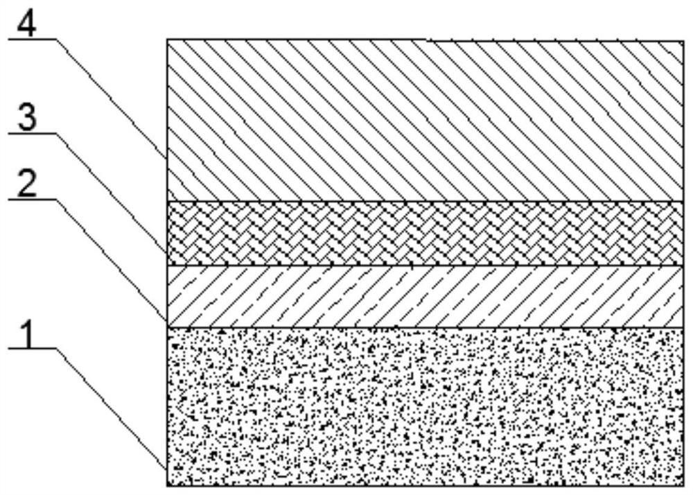
[0031] An embodiment of the present invention provides a magnetic tunnel junction, such as figure 1 As shown, it includes a reference layer 1 , a barrier layer 2 , a magnetic buffer layer 3 and a free layer 4 stacked in sequence; wherein, the ductility of the magnetic buffer layer 3 is stronger than that of the free layer 4 .
[0032] The material of the reference layer 1 is a ferromagnetic material, one or a combination of Co, Fe, CoFe, FeB, CoFeB or Heusler alloy materials can be selected, and the magnetization direction of the reference layer 1 is fixed.
[0033] The material of the barrier layer 2 is a non-magnetic material, and one or a combination of magnesium oxide, aluminum oxide, magnesium aluminum oxide, hafnium oxide, tantalum oxide, bismuth telluride or bismuth selenide can be selected things.
[0034] The material of the magnetic buffer layer 3 is also a magnetic material, and one or a combination of Co, Fe, CoFe, FeB, CoFeB or Heusler alloy materials can be sele...
Embodiment 2
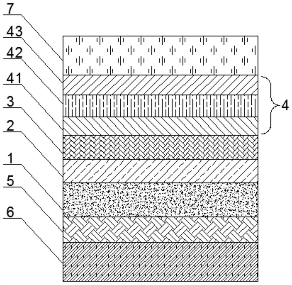
[0042] This embodiment provides a magnetic tunnel junction, such as figure 2 As shown, it includes pinning layer 6, antiferromagnetic coupling layer 5, reference layer 1, barrier layer 2, magnetic buffer layer 3 and free layer 4 stacked in sequence; wherein, the ductility of magnetic buffer layer 3 is higher than that of free layer 4 The ductility is strong. The free layer 4 includes a first free layer 41 , a coupling layer 42 and a second free layer 43 stacked in sequence. Wherein the first free layer 41 is in contact with the buffer layer. In order to protect the second free layer 43 , a cover layer 7 is further laminated on the second free layer 43 .
[0043] The material of the pinning layer 6 can be selected from one or a combination of Co, Fe, CoFe, NiFe, NiFeCo, CoFeB, CoMnB or CoNbZr.
[0044] The antiferromagnetic coupling layer 5 can be selected from one or a combination of ruthenium, chromium, rhodium or iridium.
[0045] The material of the reference layer 1 i...
Embodiment 3
[0055] This embodiment provides a method for reducing the process fluctuation of the magnetic tunnel junction free layer, including:
[0056] Provide a reference layer and a barrier layer stacked sequentially from bottom to top;
[0057] A magnetic buffer layer and a free layer are sequentially laminated on the barrier layer, and the magnetic buffer layer is more ductile than the free layer.
[0058] The specific forming process is as follows: select one or a combination of Co, Fe, CoFe, FeB, CoFeB or Heusler alloy materials as raw materials, and make the raw materials form a reference layer on the substrate.
[0059] Select one or a combination of magnesium oxide, aluminum oxide, magnesium aluminum oxide, hafnium oxide, tantalum oxide, bismuth telluride or bismuth selenide as raw materials to form a barrier layer on the reference layer .
[0060] One or a combination of Co, Fe, CoFe, FeB, CoFeB or Heusler alloy materials is selected as a raw material to form a magnetic buff...
PUM
 Abstract
Description
Claims
Application Information

