Low-gate-resistance power MOSFET device with separated gate enhancement structure and method

A technology to enhance the structure and separate the gate, which is applied in the manufacturing of electrical components, semiconductor devices, semiconductor/solid-state devices, etc., can solve the problems of large gate resistance and increase device switching loss, achieve low switching loss, reduce gate resistance value, The effect of increasing the effective cross-sectional area

Inactive Publication Date: 2021-02-26
UNIV OF ELECTRONICS SCI & TECH OF CHINA
View PDF7 Cites 3 Cited by
  • Summary
  • Abstract
  • Description
  • Claims
  • Application Information

AI Technical Summary

Problems solved by technology

However, if the control gate structure is too narrow, the gate resistance will be too large, and if the gate resistance value is too large, the switching loss of the device will be greatly increased.
[0003] Therefore, in view of the above problems, it is necessary to reduce the problem of excessive gate resistance caused by too narrow a control gate in a split gate enhancement structure, and it is against this background that the embodiments of the present invention appear

Method used


Image

  • Low-gate-resistance power MOSFET device with separated gate enhancement structure and method
  • Low-gate-resistance power MOSFET device with separated gate enhancement structure and method
  • Low-gate-resistance power MOSFET device with separated gate enhancement structure and method

Examples


Embodiment 1

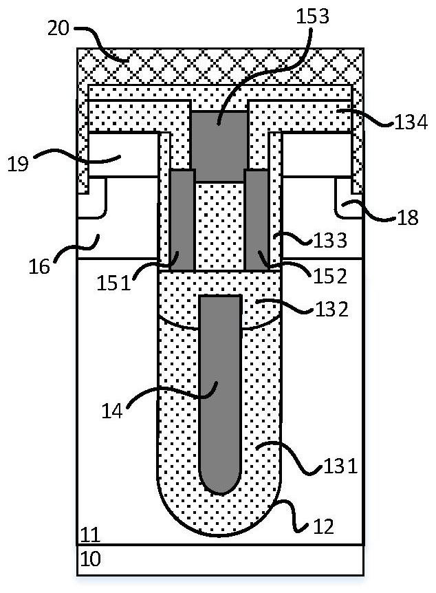
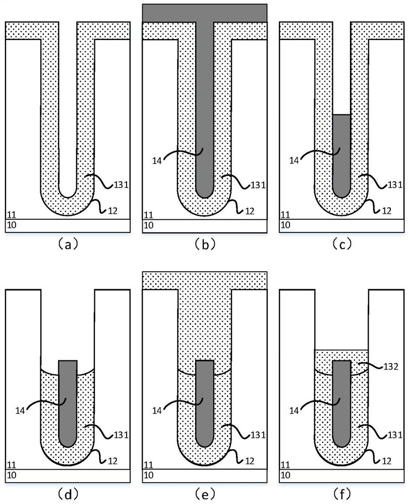
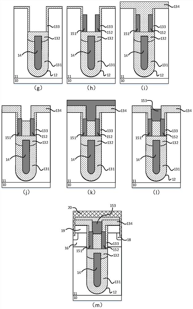
[0040] Such as figure 1As shown, a low gate resistance power MOSFET device with a split gate enhancement structure includes a first conductivity type substrate 10, a first conductivity type epitaxial layer 11 is formed on the upper surface of the first conductivity type substrate 10, and the first conductivity type epitaxial layer 11 is formed. There is a groove structure 12 in the layer 11, the groove structure 12 includes a control gate electrode and a separation gate electrode 14, the control gate electrode includes a first gate electrode 151, a second gate electrode 152 and a third gate electrode 153, the first gate electrode 151 and the separation gate electrode 14. The second gate electrode 152 is located above the separated gate electrode 14, and is separated from the separated gate electrode 14 by the second dielectric layer 132. The second conductivity type well region 16 is separated, the third gate electrode 153 is located above the first gate electrode 151 and the ...

Embodiment 2

[0055] Such as image 3 As shown, the difference between this embodiment and the structure described in Embodiment 1 is that the second dielectric layer 132 is a low-k dielectric, which can further reduce the gate-source capacitance.

Embodiment 3

[0057] Such as Figure 4 As shown, the difference between this embodiment and the structure described in Embodiment 1 is that the second dielectric layer 132 is a low-k dielectric, and the first dielectric layer 131 is a low-k dielectric, and the entire separation gate electrode is surrounded by a low-k dielectric, which can Further reduce gate-source capacitance and source-drain capacitance.


PUM


Abstract

The invention provides a low-gate-resistance power MOSFET device with a separated gate enhancement structure and a manufacturing method of the device. The low-gate-resistance power MOSFET device comprises a first conductive type substrate, a first conductive type epitaxial layer and a groove structure, the groove structure comprises a control gate electrode and a separated gate electrode, the control gate electrode comprises a first gate electrode, a second gate electrode and a third gate electrode. The third gate electrode is located above the first gate electrode and the second gate electrode and is adjacent to the first gate electrode and the second gate electrode, a second conductive type well region is located above the first conductive type epitaxial layer, and a second conductive type heavily doped region is located at the upper part of the interior of the second conductive type well region. A first conduction type heavily doped source region is arranged above the second conduction type well region. The device structure has the characteristics of low gate capacitance and low gate resistance, the aims of high switching speed and low switching loss are achieved, and a low-gate-resistance metal oxide semiconductor field effect transistor with the separated gate enhancement structure is obtained.

Description

technical field [0001] The invention belongs to the technical field of semiconductors, and more particularly relates to a low-gate-resistance split-gate enhanced power MOSFET device and a manufacturing method thereof. Background technique [0002] Power management systems require power semiconductor devices to have low on-resistance and parasitic capacitance to reduce device conduction loss and switching loss. Split-gate VDMOS has become the mainstream low-voltage device used in power management systems due to its low power loss, fast switching speed, small parasitic capacitance, and good high-frequency characteristics. The Chinese invention patent 201910191166.9 of Qiao Ming, Wang Zhengkang, Zhang Bo, etc. and the US invention patent US16 / 536333 proposed a trench MOSFET with a split gate enhancement structure, which reduces the gap between the control gate and the split gate in the split gate trench device. The parasitic capacitance Cgs and the gate charge Qg. However, if...

Claims


Application Information

Patent Timeline
Patent Type & Authority Applications(China)
IPC IPC(8): H01L29/78H01L29/423H01L21/336
CPCH01L29/7813H01L29/7809H01L29/66734H01L29/66484H01L29/4236H01L29/4238
Inventor 乔明马涛董仕达王正康张波
Owner UNIV OF ELECTRONICS SCI & TECH OF CHINA
Why Eureka
Try Eureka