Packaging structure of flexible Mini LED and preparation method of packaging structure

A packaging structure, LED lamp bead technology, applied in electrical components, electric solid devices, circuits, etc., can solve the problems of LED lamp beads being easily corroded by water vapor, poor silicone barrier ability, affecting display effects, etc., to achieve high flexible display effect, relieve stress concentration, reduce the effect of shadow area

Pending Publication Date: 2021-03-09
FUJIAN HUAJIACAI CO LTD
View PDF0 Cites 2 Cited by
  • Summary
  • Abstract
  • Description
  • Claims
  • Application Information

AI Technical Summary

Problems solved by technology

[0004] Mini LED backlight has high brightness and high power consumption compared to OLED. Currently, a reflective film is attached to the metal plate of the backlight, and the light irradiated by the LED on the metal plate is reflected to the LCD substrate through the emission film to improve the light output of the LED. Utilization rate can achieve finer high-brightness dimming; however, the cost of the reflective film is high, and posting the reflective film increases the product cost and process steps, and the Mini LED display is spliced ​​together by small-pitch LED lamp beads. The seam is unavoidable, the seam affects the display effect, and reducing the seam gap is still the future development trend;
[0005] At present, Mini LED screens are mostly driven by metal oxide TFTs, but metal oxide TFTs use IGZO films as the active layer. Coating and encapsulation, the barrier ability of silica gel to water and oxygen is poor, the side of LED lamp bead is easily eroded by water vapor, and the active layer IGZO film in the lower TFT driver is prone to device failure due to water and oxygen infection

Method used


Image

  • Packaging structure of flexible Mini LED and preparation method of packaging structure
  • Packaging structure of flexible Mini LED and preparation method of packaging structure
  • Packaging structure of flexible Mini LED and preparation method of packaging structure

Examples


preparation example Construction

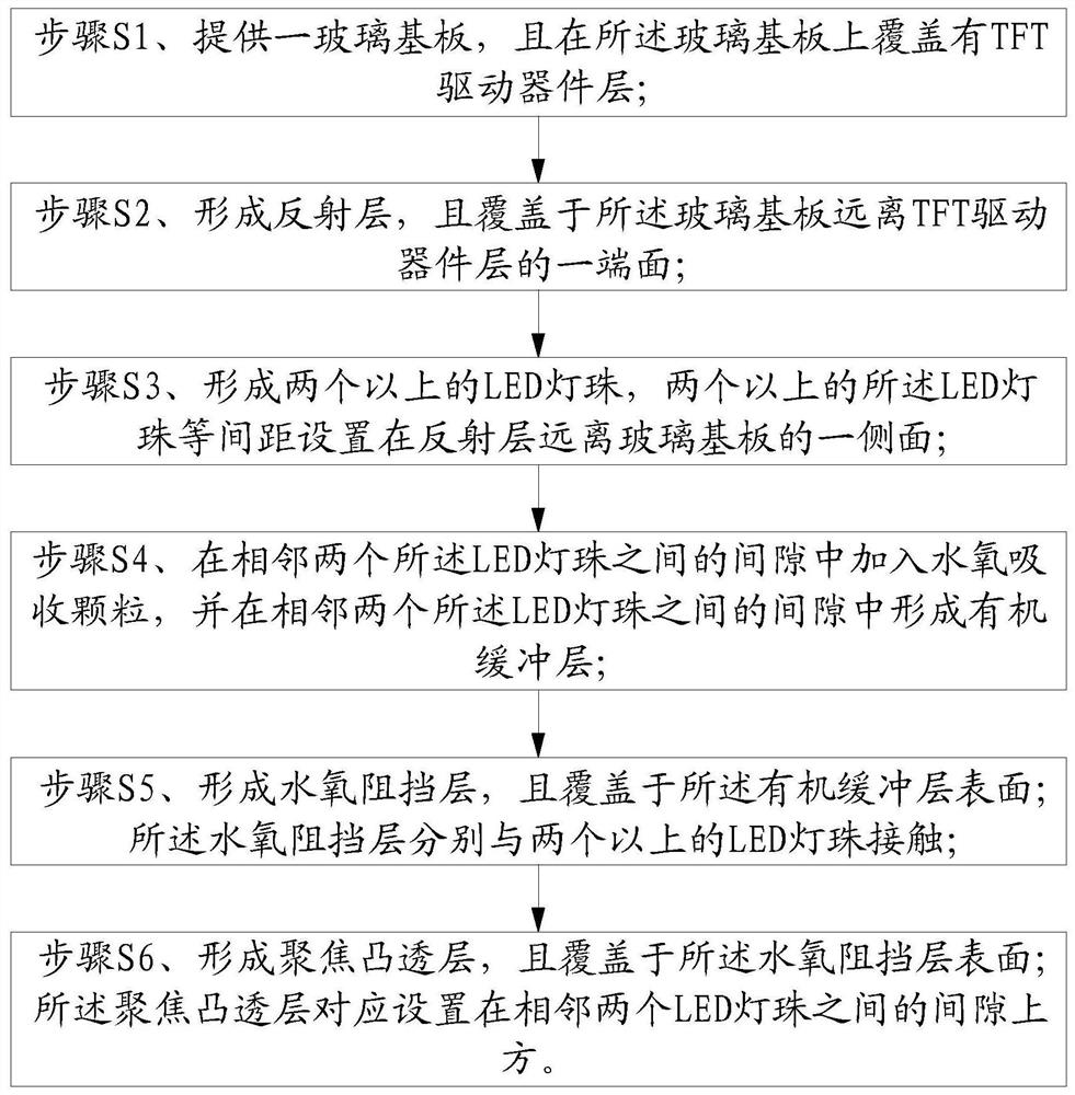
[0038] A method for preparing a packaging structure of a flexible Mini LED, comprising the following steps:

[0039] Step S1, providing a glass substrate, and a TFT driving device layer is covered on the glass substrate;

[0040] Step S2, forming a reflective layer and covering an end surface of the glass substrate away from the TFT driving device layer;

[0041] Step S3, forming more than two LED lamp beads, and the more than two LED lamp beads are arranged at equal intervals on the side of the reflective layer away from the glass substrate;

[0042]Step S4, adding water and oxygen absorbing particles in the gap between two adjacent LED lamp beads, and forming an organic buffer layer in the gap between two adjacent LED lamp beads;

[0043] Step S5, forming a water-oxygen barrier layer and covering the surface of the organic buffer layer; the water-oxygen barrier layer is respectively in contact with two or more LED lamp beads;

[0044] Step S6 , forming a focusing convex la...

Embodiment 1

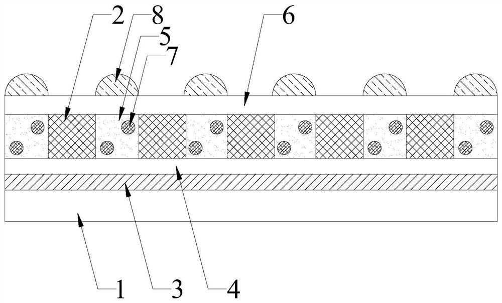
[0055] Please refer to figure 1 , Embodiment 1 of the present invention is:

[0056] A flexible Mini LED packaging structure, including a TFT driving device layer 1 and more than two LED lamp beads 2, on one end surface of the TFT driving device layer 1, a glass substrate 3, a reflective layer 4, an organic The buffer layer 5 and the water-oxygen barrier layer 6, more than two LED lamp beads 2 are embedded in the organic buffer layer 5 at equal intervals, one end surface of the LED lamp beads 2 is in contact with the water-oxygen barrier layer 6, and the One end face of the LED lamp bead 2 opposite to the other end face is in contact with the reflective layer 4, and water and oxygen absorbing particles 7 are arranged between two adjacent LED lamp beads 2, and the water and oxygen absorbing particles 7 are embedded in organic In the buffer layer 5, more than two focusing convex layers 8 are provided on the end surface of the water and oxygen barrier layer 6 away from the organ...

Embodiment 2

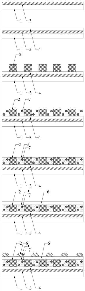
[0061] Please refer to figure 2 and image 3 , the second embodiment of the present invention is:

[0062] Please refer to figure 2 , a method for preparing a packaging structure of a flexible Mini LED, comprising the following steps:

[0063] Step S1, providing a glass substrate 3, and the TFT driving device layer 1 is covered on the glass substrate 3;

[0064] Step S2, forming a reflective layer 4, and covering an end surface of the glass substrate 3 away from the TFT driving device layer 1;

[0065] Step S3, forming more than two LED lamp beads 2, and more than two LED lamp beads 2 are arranged at equal intervals on the side of the reflective layer 4 away from the glass substrate 3;

[0066] Step S4, adding water and oxygen absorbing particles 7 in the gap between two adjacent LED lamp beads 2, and forming an organic buffer layer 5 in the gap between two adjacent LED lamp beads 2;

[0067] Step S5, forming a water-oxygen barrier layer 6 and covering the surface of th...


PUM

PropertyMeasurementUnit
thicknessaaaaaaaaaa
thicknessaaaaaaaaaa
thicknessaaaaaaaaaa

Abstract

The invention relates to the Mini LED technical field, and especially relates to a flexible Mini LED packaging structure and a preparation method thereof. The flexible Mini LED packaging structure comprises a TFT driving device layer and more than two LED lamp beads, and a glass substrate, a reflection layer, an organic buffer layer and a water oxygen barrier layer are stacked on one end face of the TFT driving device layer in sequence; more than two LED lamp beads are embedded in an organic buffer layer at equal intervals, water and oxygen absorption particles are added into gaps among the LED lamp beads, and the water and oxygen absorption particles play a role in absorbing water and oxygen permeating into the LED lamp beads, protecting the LED lamp beads and prolonging the service lifeof the LED lamp beads; more than two focusing convex transparent layers are arranged on the water-oxygen barrier layer, and the focusing convex transparent layers are correspondingly arranged above agap between two adjacent LED lamp beads, so that the brightness of the Mini LED display is improved, the shadow area at a splicing seam is reduced, and the brightness uniformity of the whole display screen is improved.

Description

technical field [0001] The invention relates to the technical field of Mini LEDs, in particular to a flexible Mini LED packaging structure and a preparation method thereof. Background technique [0002] Mini LED (English full name is mini Light Emitting Diode) is a sub-millimeter light-emitting diode. It is characterized by thinness, low power consumption, good flexibility, high bendability and good color gamut. It can finely adjust the dimming partition performance to achieve higher HDR and high contrast ratio, and can realize full-screen display devices with narrow borders, have become the focus of market attention. [0003] The Mini LED backlight technology adopts the form of flip-chip packaging, which avoids the need for secondary optical design of the lens in the traditional side-entry backlight, realizes uniform light mixing, and achieves a higher contrast effect; the backlight of the Mini LED realizes dynamic regional adjustment through the array drive Light, to achi...

Claims


Application Information

Patent Timeline
Patent Type & Authority Applications(China)
IPC IPC(8): H01L33/56H01L33/48H01L33/58H01L33/60H01L27/15
CPCH01L27/156H01L33/486H01L33/56H01L33/58H01L33/60H01L2933/0033H01L2933/005H01L2933/0058
Inventor 温质康乔小平苏智昱
Owner FUJIAN HUAJIACAI CO LTD
Why Eureka
Try Eureka