A kind of near-infrared narrow-band detector based on cadmium selenide thin film and preparation method thereof
A cadmium selenide, detector technology, used in semiconductor devices, final product manufacturing, sustainable manufacturing/processing, etc., can solve high-cost filters, surface contamination or scratches are very sensitive, commercial filters cannot meet The needs of many applications, etc., to achieve the effect of high imaging quality, low cost and simple structure
- Summary
- Abstract
- Description
- Claims
- Application Information
AI Technical Summary
Problems solved by technology
Method used
Image
Examples
preparation example Construction
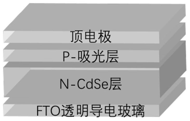
[0036] The present invention also provides a method for preparing the above-mentioned near-infrared narrow-band detector based on the cadmium selenide thin film, comprising the following steps:
[0037] (S1) Depositing a cadmium selenide film with a thickness of not less than 1 μm on the substrate;
[0038] (S2) Depositing a P-type light-absorbing layer on the cadmium selenide film;
[0039] (S3) Depositing a metal electrode on the P-type light absorbing layer, thereby obtaining a near-infrared narrow-band detector based on a cadmium selenide thin film.
[0040] In some optional embodiments, in step (S1), a cadmium selenide film is deposited on the substrate by a rapid thermal evaporation method.
[0041] In some optional embodiments, in step (S2), a P-type light absorbing layer is deposited on the cadmium selenide thin film by using a water bath deposition method or a vacuum method.
[0042] In some optional embodiments, in step (S3), metal electrodes are deposited on the P...
Embodiment 1
[0045] A method for preparing a near-infrared narrow-band detector based on a cadmium selenide thin film, comprising the steps of:
[0046](1) Clean the transparent conductive FTO glass with deionized water, acetone, isopropanol, ethanol and deionized water in turn for 30 minutes, and then dry it with a nitrogen gun to obtain a clean substrate;
[0047] (2) The cadmium selenide thin film is prepared by rapid thermal evaporation. The preparation process is to use cadmium selenide powder as the evaporation source, the vacuum degree is 1Pa, set the substrate temperature to 400°C, maintain it for 15min, and heat the evaporation source to 820°C , the evaporation time is 100s, and a cadmium selenide film with a thickness of about 2 μm is obtained;
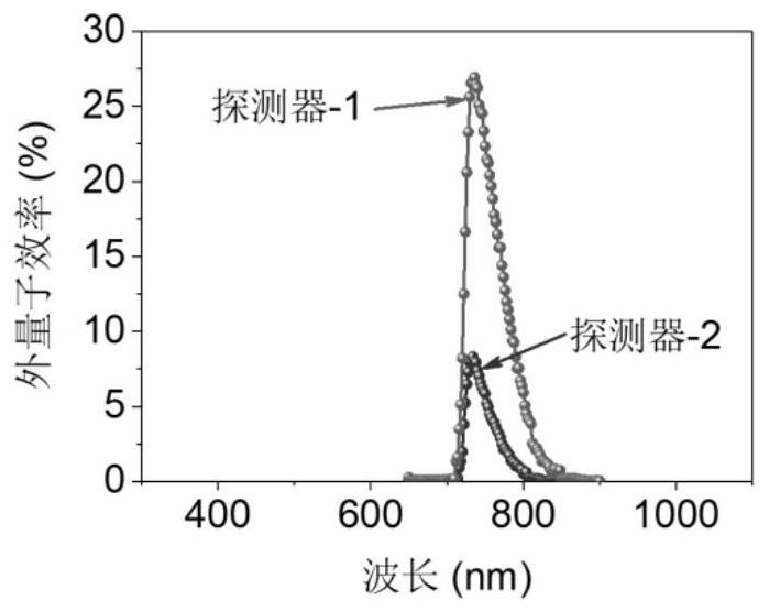
[0048] (3) Preparation of P-type Sb by water bath deposition method 2 (S, Se) 3 Light-absorbing layer, the absorption band edge is 850nm;
[0049] (4) On the P-type light-absorbing layer, metal electrodes are deposited by thermal evap...
Embodiment 2
[0052] A method for preparing a near-infrared narrow-band detector based on a cadmium selenide thin film, comprising the steps of:
[0053] (1) Clean the transparent conductive FTO glass with deionized water, acetone, isopropanol, ethanol and deionized water for 30 minutes each, and then dry it with a nitrogen gun to obtain a clean substrate;
[0054] (2) The cadmium selenide thin film is prepared by rapid thermal evaporation. The preparation process is to use cadmium selenide powder as the evaporation source, the vacuum degree is 1Pa, set the substrate temperature to 400°C, maintain it for 15min, and heat the evaporation source to 820°C , the evaporation time is 100s, and a cadmium selenide film with a thickness of about 2 μm is obtained;
[0055] (3) Preparation of P-type Sb by vacuum method 2 (S, Se) 3 Light-absorbing layer, the absorption band edge is 800nm;
[0056] (4) On the P-type light-absorbing layer, metal electrodes are deposited by thermal evaporation to prepar...
PUM
| Property | Measurement | Unit |
|---|---|---|
| thickness | aaaaa | aaaaa |
| thickness | aaaaa | aaaaa |
Abstract
Description
Claims
Application Information


