Resistive random access memory and preparation method thereof
A technology of resistive memory and dielectric layer, applied in the field of memory, can solve the problems of uneven distribution of device switching voltage, large difference in device switching voltage distribution, poor electrical performance, etc., achieve high reset voltage uniformity, reduce cumbersome The effect of improving the resistance value of high resistance state
- Summary
- Abstract
- Description
- Claims
- Application Information
AI Technical Summary
Problems solved by technology
Method used
Image

Examples
Embodiment 1
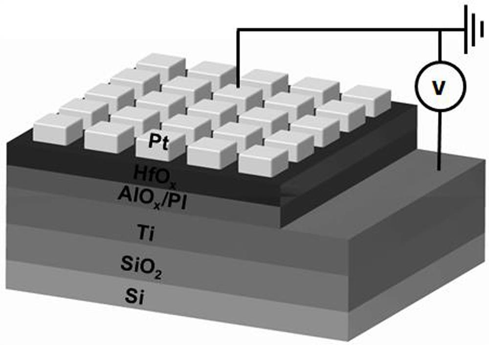
[0041] A resistive variable memory, comprising a bottom electrode, a dielectric layer and a top electrode arranged in sequence from bottom to top, the bottom electrode is preferably titanium, the dielectric layer is preferably a combination of hafnium oxide and a polyimide layer, and the top electrode is preferably Pt and Au.
[0042] A method for preparing a resistive variable memory, comprising the following steps,
[0043] (1) Si / SiO of 3 cm*3 cm 2 The slices were ultrasonically cleaned in acetone, isopropanol, and deionized water for 15 minutes each time, then dried with nitrogen and placed in a clean container;
[0044] (2) RF magnetron sputtering Ti electrode (100 nm), bulk vacuum 5*10 -4Pa, the Ar flow rate is 20 sccm, the sputtering pressure is 0.5 Pa, the sputtering power is 120 W, and the sputtering source bias is 30 V;
[0045] (3) Cut the high-temperature adhesive into two strips of 0.5 cm×3 cm in size (50% of the high-temperature adhesive is polyimide), the upp...
Embodiment 2
[0059] The difference from Example 1 is that in step (4), 4 nm aluminum oxide is firstly deposited by thermal atomic layer deposition, and then 4 nm hafnium oxide is deposited, wherein trimethylaluminum is used as the aluminum oxide source, water is used as the oxygen source, and the source is heated The temperature was 25 °C, the purge and carrier gas was nitrogen, the flow rate was 20 sccm, the temperature of the reaction chamber was 200 °C, and the thickness of the dielectric layer was 8 nm.
Embodiment 3
[0061] The difference between this example and example 1 and example 2 is that in step (4), a single layer of hafnium oxide is deposited, and the thickness of the overall dielectric layer is 8 nm.
PUM
| Property | Measurement | Unit |
|---|---|---|
| Thickness | aaaaa | aaaaa |
| Thickness | aaaaa | aaaaa |
| Thickness | aaaaa | aaaaa |
Abstract
Description
Claims
Application Information