
A kind of organic light-emitting superlattice film and its preparation method and application

A light-emitting film and superlattice technology, applied in semiconductor/solid-state device manufacturing, nanotechnology for materials and surface science, electric solid-state devices, etc., can solve problems affecting the photoelectric properties of organic superlattice and achieve excellent luminescence Effects of strength and stability, high film quality, and strong luminous brightness

Active Publication Date: 2022-03-25
NANJING UNIV
View PDF3 Cites 0 Cited by
  • Summary
  • Abstract
  • Description
  • Claims
  • Application Information

AI Technical Summary

Problems solved by technology

The island-like amorphous growth of organic thin films, the defects of organic heterojunction interfaces and other factors have a great impact on the transport properties of carriers at the interface, which in turn affects the optoelectronic properties of organic superlattices.

Method used


Image

  • A kind of organic light-emitting superlattice film and its preparation method and application
  • A kind of organic light-emitting superlattice film and its preparation method and application
  • A kind of organic light-emitting superlattice film and its preparation method and application

Examples


Embodiment 1

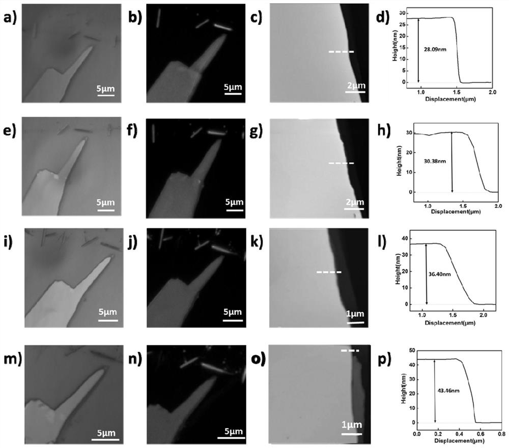
[0033] Preparation of Me-PTCDI / PTCDA / Me-PTCDI / PTCDA organic light-emitting superlattice thin films:

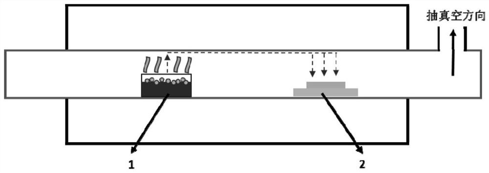
[0034] (1) Preparation of substrate: The single crystal h-BN is thinned by the traditional mechanical exfoliation method, and the thinned two-dimensional single crystal BN film is transferred to SiO with a thickness of 275nm through scotch tape. 2 a. Under the 10x objective lens through an optical microscope, a BN film with a transparent lavender color and no scotch tape residue on the surface was selected as the BN / SiO grown on the first layer of organic film 2 substrate. In this embodiment, h-BN is selected as the substrate material, because the surface of two-dimensional h-BN is flat and has no dangling bonds, and through the van der Waals interaction between two-dimensional h-BN and organic small molecules, epitaxial growth on its surface has the same flatness organic film materials.

[0035] (2) Growth of the first layer of organic luminescent film: Pour about 2.4 mg o...

Embodiment 2

[0048] The organic light-emitting superlattice film prepared in Example 1 was applied to an organic light-emitting field-effect transistor.

[0049] Using a probe, two gold electrodes with a thickness of 100nm and a length of 250μm were non-destructively transferred to the surface of the PTCDA / Me-PTCDI / PTCDA / Me-PTCDI superlattice as the source / drain electrodes of the transistor; the device was based on SiO 2 As the gate insulating layer, Si is used as the gate, and PTCDA / Me-PTCDI / PTCDA / Me-PTCDI organic light-emitting superlattice material is used as the light-emitting layer, and the following is obtained: Figure 7 An organic light-emitting field-effect transistor with the structure shown.

[0050] Because PTCDA / Me-PTCDI / PTCDA / Me-PTCDI films have extremely strong luminous intensity, they have great application prospects in the fields of display technology, optoelectronic integration, and solid-state lasers.

Embodiment 3

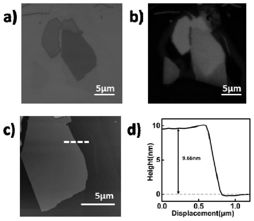
[0052] Referring to steps (1) to (2) of Example 1 to prepare Me-PTCDI organic light-emitting thin films, the difference is that in step (2), the BN / SiO 2 The substrate material was placed in the downwind area of ​​13cm in the air extraction direction, and the growth temperature of Me-PTCDI thin film was set to 217°C, and the growth time was 30min. - PTCDI organic light emitting film.

[0053]The bright field photograph under the 150 times objective lens of the optical microscope ( image 3 In (a)), we found that the surface of the transparent light purple BN substrate with a thickness below 20nm is covered with a uniform and dense dark purple region, that is, the Me-PTCDI film grown on the BN substrate. Irradiate the sample with an LED light source with a wavelength of 450nm, and the Me-PTCDI thin film area excites red fluorescence with a certain luminous brightness, such as image 3 (b) in. A high-quality layered Me-PTCDI luminescent film was prepared by this method.

[0...


PUM

PropertyMeasurementUnit
thicknessaaaaaaaaaa
thicknessaaaaaaaaaa
thicknessaaaaaaaaaa

Abstract

The invention discloses an organic light-emitting superlattice thin film, a preparation method and application thereof, and belongs to the field of organic semiconductor photoelectric materials. The organic light-emitting superlattice film is an organic light-emitting film formed by alternate epitaxial growth of two kinds of two-dimensional organic molecules on the substrate surface, and the two-dimensional organic molecules are selected from perylene-3,4,9,10-tetracarboxylic dianhydride, N,N'-Dimethyl-3,4,9,10-perylenetetracarboximide, N,N'-dioctyl-3,4,9,10-perylenedicarboximide and 3 ,4,9,10‑Tetracarboximide. The preparation method is as follows: the growth source material of the first two-dimensional organic molecule and the substrate are placed in different positions of the tube furnace, and the first layer of organic light-emitting film is epitaxially grown on the surface of the substrate; the growth source material is replaced by the second Two-dimensional organic molecules, grow the second layer of organic light-emitting thin film; repeat the replacement of growth source materials, and alternately grow multi-layer organic light-emitting thin films, that is, organic light-emitting superlattice thin films. The organic light-emitting superlattice thin film has high quality and high luminous intensity, and can be used as a light-emitting layer of an organic light-emitting field effect transistor.

Description

technical field [0001] The invention relates to a high-quality organic luminescent superlattice thin film and its preparation method and application, belonging to the technical field of organic semiconductor photoelectric materials. Background technique [0002] A superlattice is a multilayer film structure composed of two or more semiconductor layers with different energy bands that grow alternately. Thin layers of different materials grow alternately to form periodic potential wells. When the barrier width is reduced to the same scale as the mean free path of carriers, the wave functions of electrons in adjacent potential wells can overlap, and the electron movement presents a certain Wholeness. By controlling the lattice period in the superlattice to engineer the electronic bands in the material, the carrier properties of the raw material can be artificially modified. [0003] The concept of the original semiconductor superlattice was proposed in 1970 when studying nega...

Claims


Application Information

Patent Timeline
Patent Type & Authority Patents(China)
IPC IPC(8): H01L51/54H01L51/50H01L51/52H01L51/56B82Y30/00B82Y40/00
CPCB82Y40/00B82Y30/00H10K71/164H10K85/623H10K85/633H10K50/11H10K50/30H10K71/00
Inventor 王欣然陶鎏赵慧娟
Owner NANJING UNIV
Learn More