Three-dimensional memory device and forming method thereof

A three-dimensional storage and device technology, applied in semiconductor devices, electric solid state devices, electrical components, etc., can solve the problems of structural instability, storage capacity and manufacturing cost and structural stability, device size contradiction, cost increase, etc.

Active Publication Date: 2021-04-06
YANGTZE MEMORY TECH CO LTD
View PDF8 Cites 8 Cited by
  • Summary
  • Abstract
  • Description
  • Claims
  • Application Information

AI Technical Summary

Problems solved by technology

While increasing the storage capacity, it usually faces problems such as increased cost and unstable structure.
It can be seen that the existing three-dimensional memory device technology usually faces contradictions in terms of storage capacity, manufacturing cost, structural stability (or yield), and device size.

Method used


Image

  • Three-dimensional memory device and forming method thereof
  • Three-dimensional memory device and forming method thereof
  • Three-dimensional memory device and forming method thereof

Examples


Embodiment 1

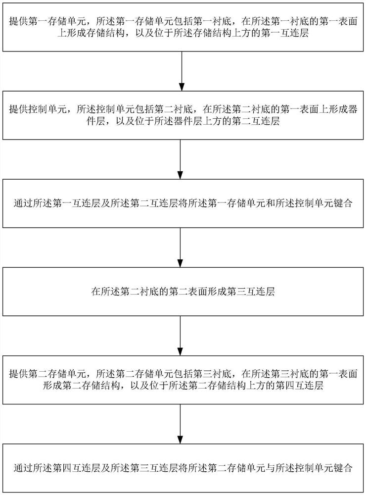
[0151]This embodiment provides a method of forming a three-dimensional memory device, such asfigure 1 As shown, the method includes the following steps:

[0152]Step S101: Provides a first storage unit including a first substrate, forming a storage structure on the first surface of the first substrate, and a first interconnection located above the storage structure. ;

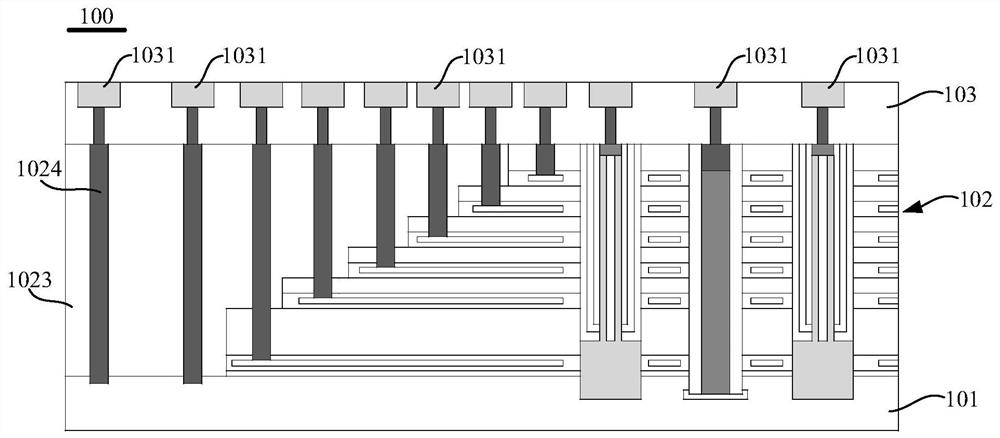
[0153]Referfigure 2 The first storage unit 100 provides a 3D NAND storage unit including a first substrate 101, a storage structure 102 is formed over the first substrate 101, and a first interconnect layer 103 is formed over the storage structure. Specifically, the following method is formed:

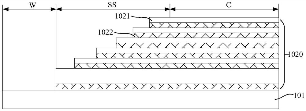
[0154]Such asimage 3 As shown, first, the first substrate 101 is provided, the first substrate having a first surface (e.g., a substrate front) and a second surface (such as a substrate back side), as an example, the first substrate 101 can be based on the actual actual Demand is selected, for example, may include a silicon substrate,...

Embodiment 2

[0185]This embodiment also provides a method of forming a three-dimensional memory device, and is not described in the same manner as the first example, and the difference is:

[0186]ReferFigure 12 In this embodiment, the source layer of the array is stored in the array of arrays.Front connectionTo the control circuit of the control unit, the array co-source contact is not repeated from the second surface of the first substrate and / or the third substrate. In this embodiment, the source layer can achieve a connection between the source layer and the control unit by the peripheral contact 402 formed in the substrate of the first storage unit and the second memory cell. Or in an alternative embodiment, here referencefigure 2 Further, the first contact 1031 formed at the top of the common source line 105 is in contact with the top cycle, and the source layer is connected to the control unit by a common source line, and the front side of the source layer is connected to the control unit ...

Embodiment 3

[0190]This embodiment also provides a method of forming a three-dimensional memory device, and is not described in the same place as in Example 2, and the difference is:

[0191]Such asFigure 13 As shown in the present embodiment, the back surface of the substrate of the first substrate 101 of the first storage unit 100 does not form a contact pad, and a contact pad 502 is formed only on the back surface of the third substrate 301. The array source layer of the memory cell and the leader of the control unit are realized by contact pad 502.

[0192]This embodiment is also providedFigure 13 The three-dimensional memory device shown. The memory device implements the storage unit and the leader of the control unit at a lower number of pads, which facilitates the integration of the device.


PUM


Abstract

The invention provides a three-dimensional memory device and a forming method thereof. A memory unit is bonded with a control unit, and then another memory unit is bonded on the back surface of a substrate of the control unit, so that bonding of at least three units is realized. Therefore, wafer-level bonding is realized, the process is simpler, the stress problem can be effectively solved while the number of storage layers is increased, the structure is more stable, and the risk of structural collapse is reduced. After the memory unit and the control unit are bonded, the bonding pads on the two sides are led out, the bonding pads can be led out from the sides of the two memory units, the bonding pads can also be led out from the two sides of one memory unit and the two sides of the control unit, and a control circuit of the control unit is used for controlling the memory unit accessed during memory. The pad leading-out mode is added, and the number of bonding pads per unit area is increased. The number of bonding pads per unit area is increased, the access hit rate of the memory unit can be improved, and therefore the memory period of the memory unit can be greatly shortened.

Description

Technical field[0001]The present invention relates to the field of semiconductor integrated circuit manufacturing, and more particularly to a three-dimensional memory device and a method of forming thereof.Background technique[0002]As the characteristic size of the device in the integrated circuit is constantly narrowing, a plurality of planes of memory cells are stacked to achieve greater storage capacity and implement three-dimensional memory technology per bit lower cost is more favored.[0003]The three-dimensional memory device is usually facing the problem of storage capacity and cost, the pads of the pads and the stress problem. For storage capacity and cost issues, the storage capacity of the memory device is typically increased by increasing the amount of storage of each memory cell, or the storage unit is minimized, to increase the storage capacity of the unit area. While increasing storage capacity, it usually faces problems with increased cost, structural instability. It c...

Claims


Application Information

Patent Timeline
Patent Type & Authority Applications(China)
IPC IPC(8): H01L27/1157H01L27/11573H01L27/11582
CPCH10B43/40H10B43/35H10B43/27
Inventor 张坤周文犀夏志良
Owner YANGTZE MEMORY TECH CO LTD
Why Eureka
Try Eureka