Back gate full-controlled AlGaN/GaN heterojunction enhanced power HEMT device and preparation method thereof
A fully-controlled, heterojunction technology, which is applied in semiconductor/solid-state device manufacturing, semiconductor devices, electrical components, etc., can solve the problems of gate electrode leakage current and breakdown voltage, etc., and achieves good threshold voltage stability and improved The effect of enhanced breakdown voltage and gate control ability
- Summary
- Abstract
- Description
- Claims
- Application Information
AI Technical Summary
Problems solved by technology
Method used
Image
Examples
Embodiment 1
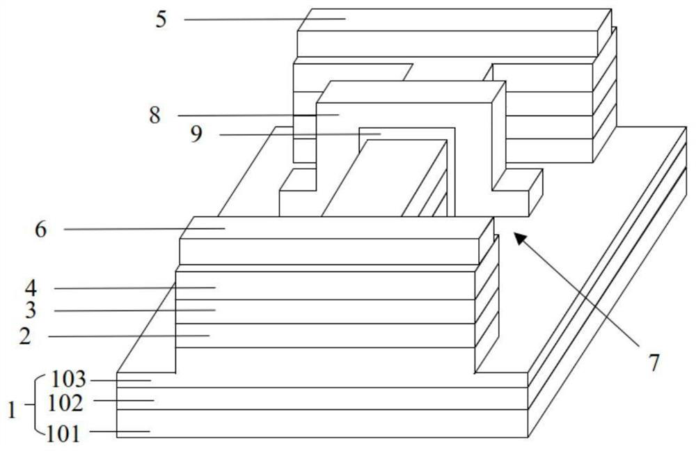
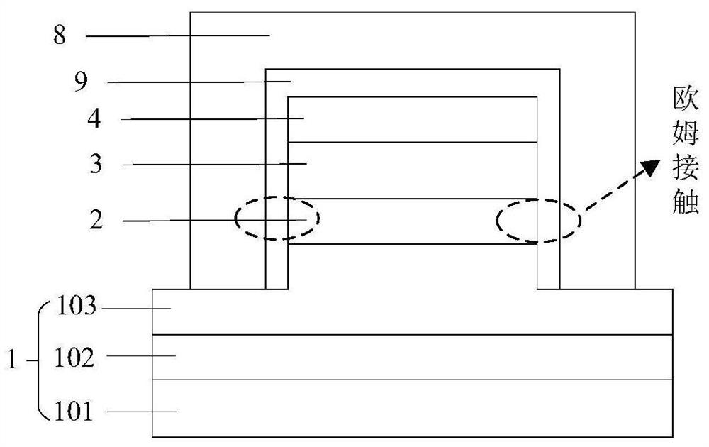
[0040] Please refer to figure 1 and figure 2 , figure 1 It is a three-dimensional structure diagram of a back-gate fully-controlled AlGaN / GaN heterojunction enhanced power HEMT device provided by an embodiment of the present invention; figure 2 It is a cross-sectional view of a back-gate fully-controlled AlGaN / GaN heterojunction enhanced power HEMT device provided by an embodiment of the present invention. As shown in the figure, the back-gate fully controlled AlGaN / GaN heterojunction enhancement mode power HEMT device of this embodiment includes: a substrate 1, a P-GaN layer 2, a GaN channel layer 3, an AlGaN barrier layer 4, Source electrode 5 , drain electrode 6 , gate electrode 8 and gate dielectric layer 9 . The substrate 1 , the P-GaN layer 2 , the GaN channel layer 3 and the AlGaN barrier layer 4 are sequentially stacked from bottom to top. The source electrode 5 is arranged on one side of the AlGaN barrier layer 4 , and the drain electrode 6 is arranged on the ot...
Embodiment 2
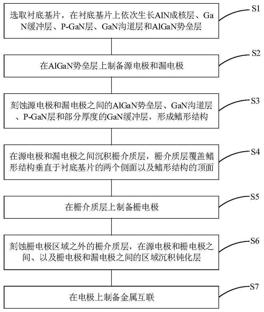
[0051] This embodiment provides a method for fabricating a back-gate fully controlled AlGaN / GaN heterojunction enhancement mode power HEMT device. Please refer to image 3 image 3 It is a schematic diagram of a preparation method of a back-gate fully-controlled AlGaN / GaN heterojunction enhanced power HEMT device provided by an embodiment of the present invention. As shown in the figure, the method includes:
[0052] S1: select a substrate substrate, and sequentially grow an AlN nucleation layer, a GaN buffer layer, a P-GaN layer, a GaN channel layer and an AlGaN barrier layer on the substrate substrate;
[0053] S2: source and drain electrodes are prepared on the AlGaN barrier layer;
[0054] S3: Etch the AlGaN barrier layer, the GaN channel layer, the P-GaN layer and the partial thickness of the GaN buffer layer between the source electrode and the drain electrode to form a fin-shaped structure;
[0055] S4: depositing a gate dielectric layer between the source electrode a...
PUM
| Property | Measurement | Unit |
|---|---|---|
| thickness | aaaaa | aaaaa |
| thickness | aaaaa | aaaaa |
| width | aaaaa | aaaaa |
Abstract
Description
Claims
Application Information


