Formation method of semiconductor structure

A semiconductor and tunnel junction technology, applied in the field of semiconductor structure formation, can solve the problems of ultra-deep lateral current spreading limitation, difficulty in deep implantation of ions, long implantation time, etc. Effect

Active Publication Date: 2021-06-18
度亘核芯光电技术(苏州)有限公司
View PDF4 Cites 0 Cited by
  • Summary
  • Abstract
  • Description
  • Claims
  • Application Information

AI Technical Summary

Problems solved by technology

[0005] The purpose of the present invention is to provide a method for forming a semiconductor structure to solve the problem of limitation of ultra-deep lateral current extension, and at the same time alleviate the technical problems of the existing ion implantation method, such as difficulty in implanting ions deeply, shallow implantation depth and long implantation time

Method used


Image

  • Formation method of semiconductor structure
  • Formation method of semiconductor structure
  • Formation method of semiconductor structure

Examples


Embodiment Construction

[0040] The technical solutions of the present invention will be clearly and completely described below in conjunction with the embodiments. Obviously, the described embodiments are part of the embodiments of the present invention, but not all of them. Based on the embodiments of the present invention, all other embodiments obtained by persons of ordinary skill in the art without making creative efforts belong to the protection scope of the present invention.

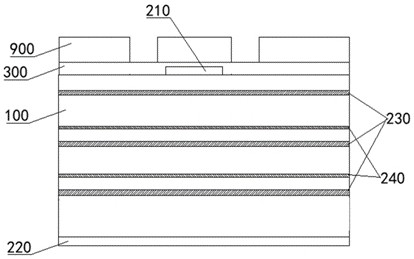
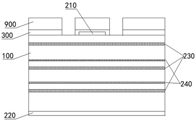
[0041] like Figure 2-Figure 10 As shown, the method for forming the semiconductor structure 100 provided by the embodiment of the present invention includes the following steps:

[0042] S1. Form a mask structure 300 on the upper surface of the semiconductor structure 100 and perform etching to form an opening on the mask structure 300 .

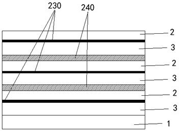
[0043] like figure 2 and image 3 As shown, the thickness of the mask structure 300 may be greater than that of the upper electrode 210 , so as to cover the upper electrode 210 and ...


PUM

PropertyMeasurementUnit
thicknessaaaaaaaaaa

Abstract

The invention provides a method for forming a semiconductor structure, which relates to the technical field of semiconductor processing. The method for forming a semiconductor structure includes the following steps: S1. Form a mask structure on the upper surface of the semiconductor structure, and after etching, Form an opening on the mask structure; S2. Through the opening, use etching plasma gas to etch the semiconductor structure at the bottom of the mask structure to form an upper trench structure, and the bottom edge region and sides of the upper trench structure formed by etching The wall is formed with organic residues; S3. Etching the bottom of the upper trench structure to form a lower trench structure; wherein, the width of the lower trench structure is smaller than the width of the upper trench structure; S4. In the upper trench structure and the lower trench Ion implantation is carried out in the trench structure to form a high resistance region.

Description

technical field [0001] The invention relates to the technical field of semiconductor processing, in particular to a method for forming a semiconductor structure. Background technique [0002] The lateral expansion of injection current is one of the core issues that affect the power boost and luminous width control of high-power edge-emitting semiconductor devices. [0003] Common methods for current lateral expansion limitation include methods such as introducing deep isolation trenches through etching (corrosion) or ion implantation to form high-resistance regions in the manufacturing process. Among them, ion implantation is proved to have special advantages in power enhancement and near-field spot limitation due to its small loss and no obvious lateral expansion problem, and at the same time, it can reduce the accumulation effect of carriers at the edge of the implanted region. [0004] like figure 1 As shown, in the prior art, the double tunnel junction structure includ...

Claims


Application Information

Patent Timeline
Patent Type & Authority Patents(China)
IPC IPC(8): H01L33/00H01L33/06H01L33/14
CPCH01L33/0062H01L33/06H01L33/14
Inventor 杨国文唐松
Owner 度亘核芯光电技术(苏州)有限公司
Why Eureka
Try Eureka