

Design and manufacturing method of high-power ultraviolet LED chip with vertical structure
A LED chip and vertical structure technology, applied in semiconductor devices, electrical components, circuits, etc., can solve the problems of small size, high manufacturing cost, and low luminous efficiency
- Summary
- Abstract
- Description
- Claims
- Application Information
AI Technical Summary
Problems solved by technology
Method used
Image

Examples
Embodiment
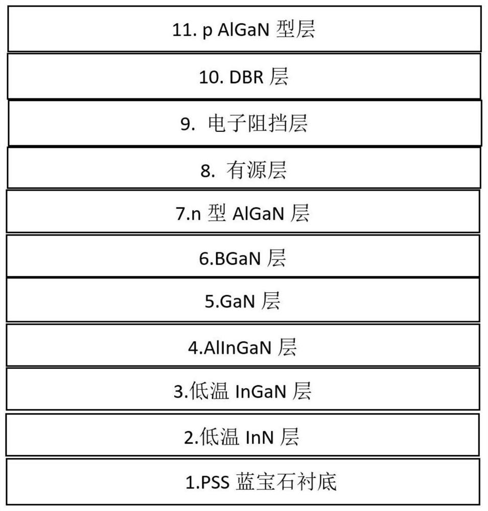
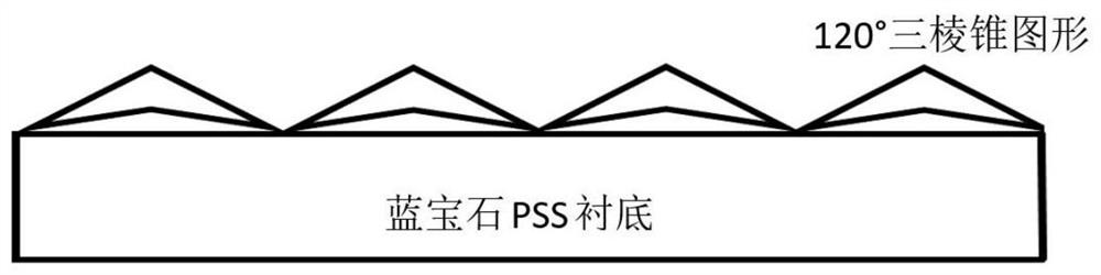
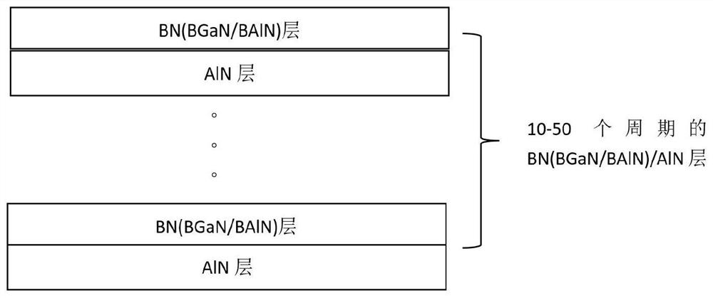
[0033] see Figure 1-5 , the present invention provides a technical solution: a design and manufacturing method of a high-power vertical structure ultraviolet LED chip, the design of the high-power vertical structure ultraviolet LED chip is as follows: a sapphire substrate is used as a growth substrate for heteroepitaxial growth, Using MOCVD technology to complete the entire epitaxial process, the sapphire substrate adopts an image substrate, that is, a PSS substrate. This substrate adopts a special design, which is a triangular pyramid structure with a vertex angle of 120°. A thin layer of low-temperature InN is grown on the PSS. Then grow a layer of InGaN, then grow a thin layer of AlGaInN, then grow a layer of high-temperature GaN, then grow a layer of n-type AlGaN, then grow an active layer, an electron blocking layer, and then grow a DBR reflective layer. The DBR layer is 10-50 BAlN or BGaN or BN and AlN periodic structure layers, doped with magnesium source and less sila...
PUM
| Property | Measurement | Unit |
|---|---|---|
| diameter | aaaaa | aaaaa |
| diameter | aaaaa | aaaaa |
Abstract
Description
Claims
Application Information