Method for cleaning etched semiconductor wafer

A semiconductor and post-cleaning technology, which is applied in the direction of cleaning methods using liquids, cleaning methods and utensils, semiconductor/solid-state device manufacturing, etc., can solve problems such as difficult to completely remove products and affect chip performance, and achieve strong repeatability. Avoid static electricity and simple operation process

Active Publication Date: 2021-05-14
NO 55 INST CHINA ELECTRONIC SCI & TECHNOLOGYGROUP CO LTD
View PDF5 Cites 2 Cited by
  • Summary
  • Abstract
  • Description
  • Claims
  • Application Information

AI Technical Summary

Problems solved by technology

Regardless of front pattern etching, mesa isolation or back deep hole etching, etc., the by-products produced after etching have a fatal impact on the performance of the chip. If they cannot be removed, they will directly affect the performance, yield and reliability of the product; The by-products produced after etching are closely related to the material composition and etching gas. The existing cleaning methods can effectively remove a small amount of by-products produced by etching, but they are not suitable for large-area mesa, higher steps and deep holes. It is difficult to completely remove a large amount of products after etching, so it is particularly important to completely remove these etching by-products

Method used


Image

  • Method for cleaning etched semiconductor wafer

Examples


Embodiment 1

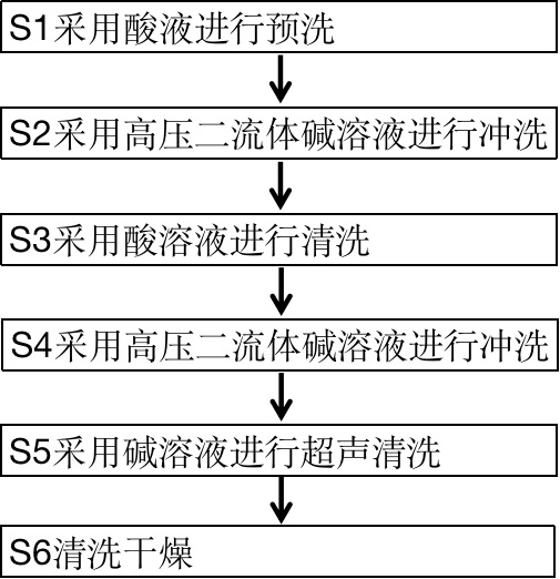
[0067] A method for cleaning a GaN semiconductor wafer after etching, characterized in that the cleaning method comprises the following steps:

[0068] S1 is pre-washed with acid solution; the acid pre-wash solution includes nitric acid, ozone and water, the temperature is 75 ° C, ultrasonic cleaning is used, and the frequency is 230KHz;

[0069] S2 is flushed with a high-pressure two-fluid alkaline solution; the high-pressure two-fluid alkaline cleaning solution contains sodium hydroxide and water, the volume ratio is 1.5:135, and the high pressure is 125 PSI, and the alkaline solution is used in the form of two fluids during the flushing process. Wafers are rinsed;

[0070] S3 is cleaned with an acid solution; the acid cleaning solution contains sulfuric acid, hydrogen peroxide and water at a temperature of 128°C, and ultrasonic cleaning is used at a frequency of 650KHz.

[0071] S4 uses a high-pressure two-fluid alkaline solution to rinse; the high-pressure alkaline cleani...


PUM


Abstract

The invention discloses a method for cleaning an etched semiconductor wafer. The method comprises the following steps: 1, pre-cleaning the semiconductor wafer by using acid liquor; 2, washing with a high-pressure two-fluid alkaline solution; 3, cleaning with an acid solution; 4, washing with the high-pressure two-fluid alkali solution; 5, carrying out ultrasonic cleaning through an alkali solution; and 6, cleaning and drying. The semiconductor wafer can be thoroughly cleaned after being etched, and the method has the advantages of being simple and convenient in operation process, high in repeatability and the like, and can be suitable for large-scale industrial production.

Description

technical field [0001] The invention belongs to the technical field of semiconductor cleaning, and in particular relates to a method for cleaning semiconductor wafers after etching. Background technique [0002] With the continuous development of semiconductors and their wide application fields, the performance requirements are getting higher and higher. As a key supporting technology, etching technology is indispensable in the semiconductor process, which determines the performance of the chip to some extent. For example, the backside through hole process in the semiconductor process can effectively reduce the source grounding inductance and increase heat dissipation Performance is regarded as a key process. Regardless of front pattern etching, mesa isolation or back deep hole etching, etc., the by-products produced after etching have a fatal impact on the performance of the chip. If they cannot be removed, they will directly affect the performance, yield and reliability o...

Claims


Application Information

Patent Timeline
Patent Type & Authority Applications(China)
IPC IPC(8): H01L21/02B08B3/02B08B3/08
CPCH01L21/02057B08B3/02B08B3/08Y02P70/50
Inventor 李彭瑞任春江潘斌陈堂胜
Owner NO 55 INST CHINA ELECTRONIC SCI & TECHNOLOGYGROUP CO LTD
Why Eureka
Try Eureka