Schottky diode based on silicon carbide planar MOS structure

A technology of Schottky diode and MOS structure, which is applied in the direction of electrical components, circuits, semiconductor devices, etc., can solve serious problems such as leakage current, and achieve the effects of reducing gate-channel ratio, reducing switching loss, and reducing on-resistance

Active Publication Date: 2021-05-25
JIANGSU HAIDONG SEMICON TECH CO LTD
View PDF5 Cites 2 Cited by
  • Summary
  • Abstract
  • Description
  • Claims
  • Application Information

AI Technical Summary

Problems solved by technology

[0003] Silicon carbide Schottky diodes have a majority of conductive carriers. When a forward bias is applied, the silicon carbide Schottky diodes have a low turn-on voltage. When the applied voltage switches from forward conduction to reverse blocking, there is almost no reverse Recovery current can recover quickly, but under reverse bias, due to the Schottky barrier reduction effect, serious leakage current phenomenon will occur

Method used


Image

  • Schottky diode based on silicon carbide planar MOS structure

Examples


Embodiment Construction

[0015] The following will clearly and completely describe the technical solutions in the embodiments of the present invention with reference to the accompanying drawings in the embodiments of the present invention. Obviously, the described embodiments are only some, not all, embodiments of the present invention. Based on the embodiments of the present invention, all other embodiments obtained by persons of ordinary skill in the art without making creative efforts belong to the protection scope of the present invention.

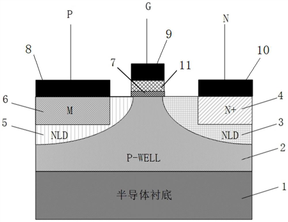
[0016] Such as figure 1 As shown: in order to effectively reduce the switching loss of the semiconductor device and increase its switching speed, the switch of the Schottky diode controlled by the MOS gate channel can also be realized, thereby improving the electrical performance of the Schottky diode. In the embodiment of the present invention, On the cross-section of the Schottky diode, it includes a semiconductor substrate 1 and a P-type well region 2 dispo...


PUM


Abstract

The invention relates to a semiconductor device, in particular to a Schottky diode based on a silicon carbide planar MOS structure. According to the technical scheme provided by the invention, the Schottky diode based on the silicon carbide planar MOS structure comprises a semiconductor substrate and a P-type well region arranged on the semiconductor substrate on the cross section of the Schottky diode, a negative electrode region structure is arranged on one side of the P-type well region, a positive electrode region structure is arranged on the other side of the P-type well region, the P-type well region is in contact with a gate structure region located on the P-type well region, gate metal is arranged on the gate structure region, and the gate metal is in ohmic contact with the gate structure region. According to the invention, the switching loss of the semiconductor device is effectively reduced, the switching speed of the semiconductor device is improved, the switching of the Schottky diode can be controlled by the MOS gate channel, and the electrical performance of the Schottky diode is further improved.

Description

technical field [0001] The invention relates to a semiconductor device, in particular to a Schottky diode based on a silicon carbide planar MOS structure. Background technique [0002] Silicon carbide (SiC) material has the advantages of large band gap, high critical breakdown field strength, high thermal conductivity, high saturated electron drift velocity and low dielectric constant, and is widely used in high frequency, high power, high temperature resistance, Anti-radiation and other electronic devices. [0003] Silicon carbide Schottky diodes have a majority of conductive carriers. When a forward bias is applied, the silicon carbide Schottky diodes have a low turn-on voltage. When the applied voltage switches from forward conduction to reverse blocking, there is almost no reverse The reverse recovery current can recover quickly, but due to the Schottky barrier lowering effect under reverse bias, a serious leakage current phenomenon will occur. Contents of the inventi...

Claims


Application Information

Patent Timeline
Patent Type & Authority Applications(China)
IPC IPC(8): H01L29/872H01L29/06
CPCH01L29/872H01L29/0607
Inventor 夏华忠黄传伟李健诸建周吕文生谈益民
Owner JIANGSU HAIDONG SEMICON TECH CO LTD
Why Eureka
Try Eureka