Supercharge Your Innovation With Domain-Expert AI Agents!

Method for forming conductive layer using atomic layer deposition process

An atomic layer, silicon atom technology, applied in metal material coating process, coating, circuit and other directions, can solve the problems of increased silicon loss, difficulty in forming a titanium silicide layer, and inferior junction leakage characteristics.

Inactive Publication Date: 2003-11-19
SAMSUNG ELECTRONICS CO LTD
View PDF0 Cites 0 Cited by
  • Summary
  • Abstract
  • Description
  • Claims
  • Application Information

AI Technical Summary

Problems solved by technology

However, when the titanium silicide layer is formed at a temperature of 600°C or higher, the loss of silicon in the doped layer in contact with the silicon layer will increase, deteriorating the characteristics of junction leakage
Therefore, for highly integrated semiconductor devices that require shallow junctions, it is difficult to form a titanium silicide layer by LPCVD.

Method used


Image

  • Method for forming conductive layer using atomic layer deposition process
  • Method for forming conductive layer using atomic layer deposition process
  • Method for forming conductive layer using atomic layer deposition process

Examples


Embodiment Construction

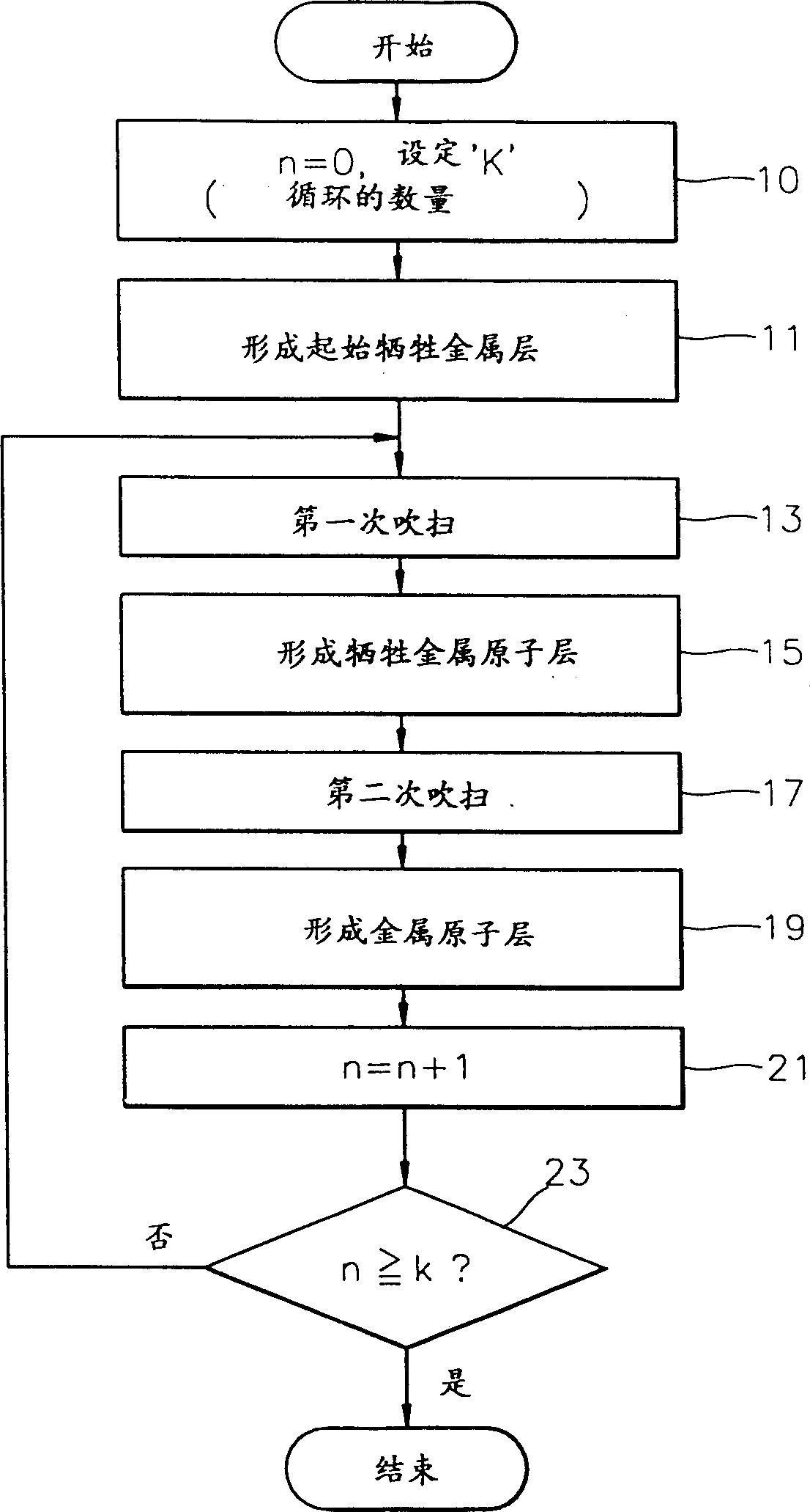
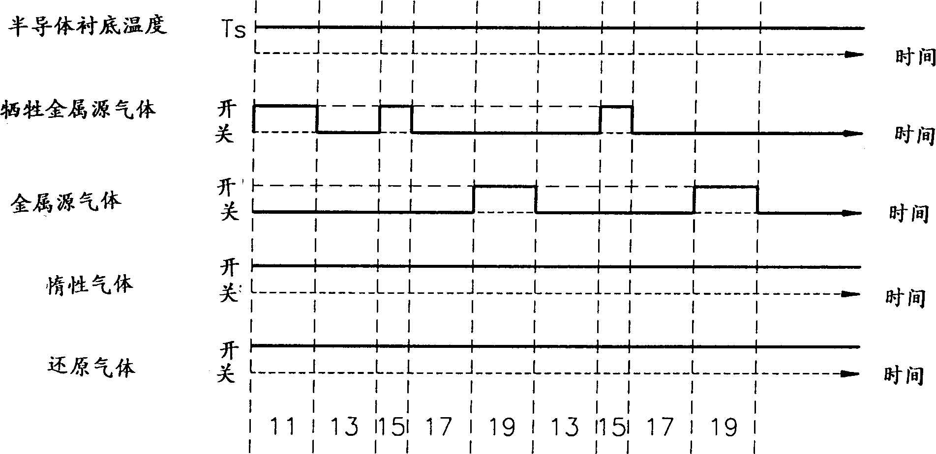
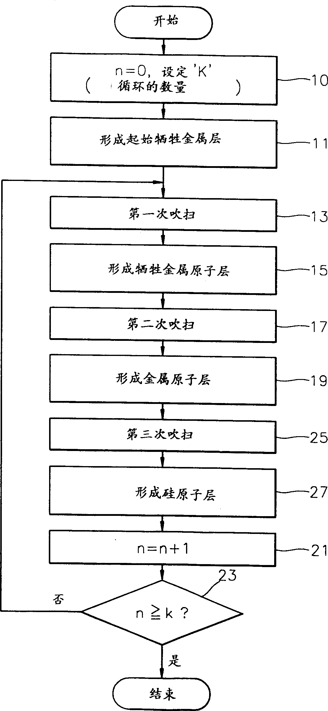
[0020] see Figure 5 , The device for forming the conductive layer according to the present invention includes a reaction chamber 51, a susceptor 53 installed at the bottom of the reaction chamber 51 for positioning a semiconductor substrate 55 on top of the susceptor 53, and mounted on the susceptor 53 for facing the reaction chamber 51. A shower head 57 for injecting reaction gas, and a vacuum rod 59 connected with the reaction chamber 51 to control the pressure in the reaction chamber 51. In the present invention, the shower head 57 includes two gas inlets A and B separated from each other. The metal source gas and the inert gas are injected into the reaction chamber 51 through the gas inlet A, and the silicon source gas, the sacrificial metal source gas and the reducing gas are injected into the reaction chamber 51 through the gas inlet B. This makes it possible to confine the reaction of the gas to one of the inlets A and B before reaching the reaction chamber 51 . The ...


PUM


Abstract

A method for forming conductive layer using atomic layer deposition process reacts a precursor containing metal with a reducing gas, forming a metal atom on a semiconductor substrate and a position deposited metal atoms dissolved by metal halide gas by reacting a sacrificial metal atoms layer with metal halide gas. Moreover, a silicon layer may be additionally formed on the metal layer using a silicon source gas, to thereby alternately stack metal layers and silicon layers.

Description

technical field [0001] The present invention relates to a method for forming a conductive layer on a semiconductor device, in particular to a method for forming a conductive layer by atomic layer deposition. Background of the invention [0002] As the integration of conductor arrangements increases, the design rules decrease. Therefore the aspect ratio of the contact hole becomes higher, however, the junction depth becomes shallower. The junction depth directly depends on the short channel effect of the MOS transistor. That is to say, MOS transistors suitable for highly integrated semiconductor devices require shorter trench lengths and shallow source / drain region depths, that is, shallow junction depths to improve the characteristics of MOS transistors with short trenches. Interconnection techniques for accessing shallow junctions through metal interconnections require a barrier metal layer. This hinders penetration of metal interconnects into shallow junctions, ie preve...

Claims


Application Information

Patent Timeline
IPC IPC(8): C23C16/08C23C16/42C23C16/44C23C16/455H01L21/285H01L21/768
CPCH01L21/28518C23C16/44C23C16/45561H01L21/28556C23C16/45534C23C16/42H01L21/76838C23C16/08
Inventor 姜尚范蔡允淑朴昌洙李相忍
Owner SAMSUNG ELECTRONICS CO LTD
Features
  • R&D
  • Intellectual Property
  • Life Sciences
  • Materials
  • Tech Scout
  • Unparalleled Data Quality
  • Higher Quality Content
  • 60% Fewer Hallucinations
Learn More