Metal and dielectric compounded high-temperature-resistant solar spectrum selective absorption structure
A dielectric composite, solar spectrum technology, applied in the field of high temperature resistant solar spectrum selective absorption structure, can solve the problems of narrow absorption spectrum range, complex structure, oxidation failure, etc., achieve design diversification, prevent diffusion and oxidation, good high temperature resistance performance effect
- Summary
- Abstract
- Description
- Claims
- Application Information
AI Technical Summary
Problems solved by technology
Method used
Image
Examples
Embodiment 1
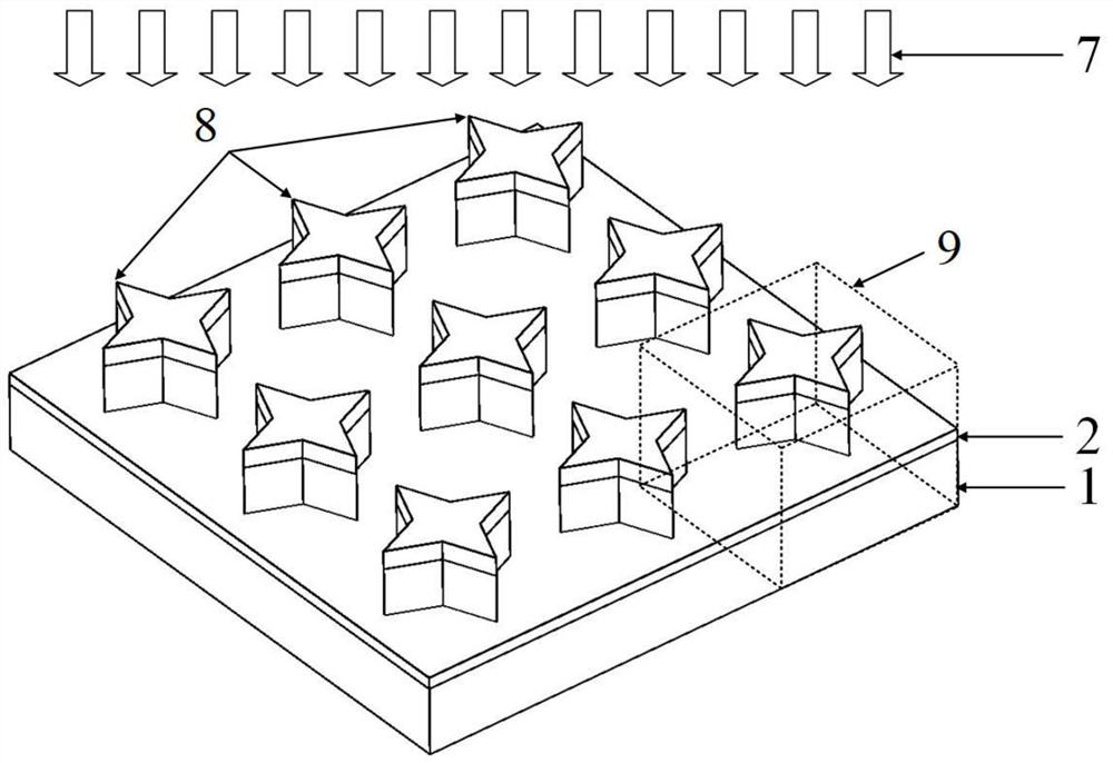
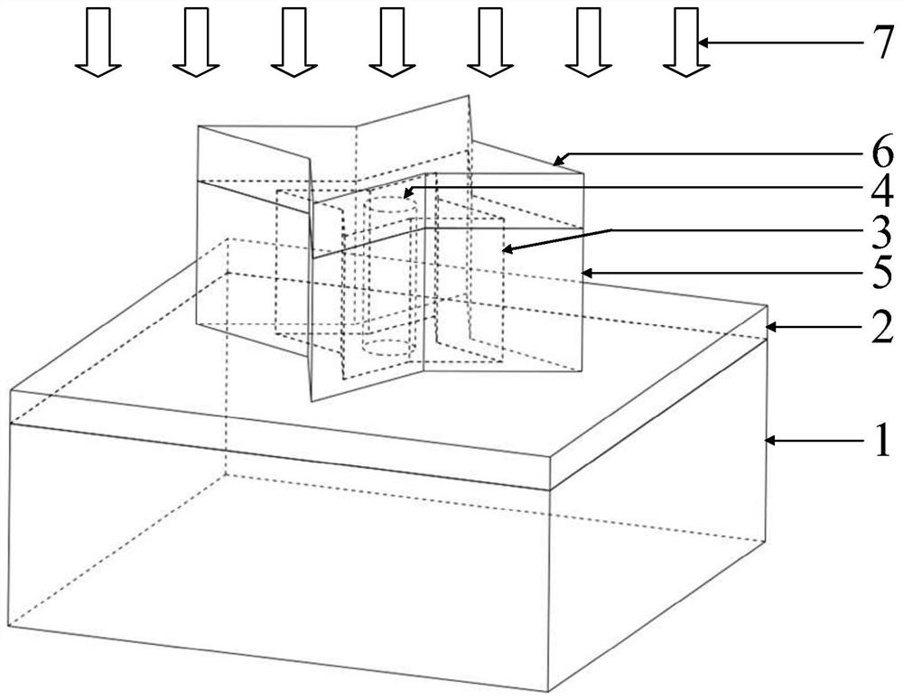
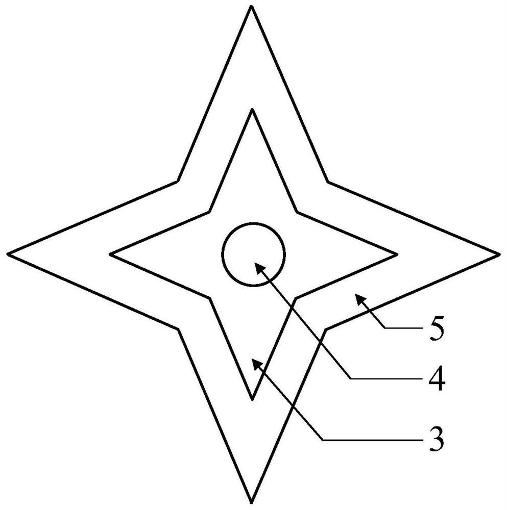
[0037] The material of the underlying metal film 1 is tungsten, with a thickness of 240nm; the metal nano-square star prisms 3 with cylindrical holes in the center are arranged in a square (i.e. a special parallelogram) array, and two adjacent metal nano-square star prisms The distance of the central axis of the prism 3 corresponds to the side length of the square, and its value is 476nm; the material of the metal nano-square star-shaped prism 3 is tungsten, and the thickness of each metal nano-square star-shaped prism 3 is 170nm. A four-pointed star with a circular hole, wherein the diameter of the circumscribed circle of the four-pointed star is 280nm, the diameter of the central circular hole is 60nm, and the degree of each angle is 46.4°; the dielectric filler 4, the first dielectric film 2, the second dielectric film 5, the second The materials of the three dielectric thin films 6 are all made of hafnium dioxide, and their thicknesses are 170nm, 40nm, 38.6nm and 65nm respe...
Embodiment 2
[0051] The material of the underlying metal film 1 is tungsten, and the thickness is 230nm; the metal nano-square star-shaped prism 3 with a cylindrical hole in the center is arranged in a regular hexagonal array, and the minimum distance between the central axes of two adjacent metal nano-square star-shaped prisms 3 Corresponding to the side length of a regular hexagon, its value is 550nm; the material of the metal nano-square star-shaped prism 3 is tungsten, and the thickness of each metal nano-square star-shaped prism 3 is 180nm, and its cross section is a four-pointed star with a round hole in the center. , wherein the diameter of the circumscribed circle of the four-pointed star is 300nm, the diameter of the central circular hole is 65nm, and the degree of each angle is 48°; the dielectric filler 4, the first dielectric film 2, the second dielectric film 5, and the third dielectric film 6 All materials use HfO 2 , and their thicknesses are 180nm, 50nm, 40nm, and 65nm, res...
Embodiment 3
[0053] The material of the underlying metal film 1 is chromium, and the thickness is 200nm; the metal nano-square star prism 3 with a cylindrical hole in the center is arranged in a rhombus (a special parallelogram) array, and two adjacent metal nano-square star prisms 3 The minimum distance between the central axes of the rhombus corresponds to the side length of the rhombus, and its value is 530nm; the two smaller angles of the rhombus are both 80°, and the two larger angles are both 100°. The metal nano-square star-shaped prism 3 is made of chromium, and the thickness of each metal nano-square star-shaped prism 3 is 185nm. The diameter of the hole is 50nm, and the degree of each angle is 45°; the materials of the dielectric filler 4, the first dielectric film 2, the second dielectric film 5, and the third dielectric film 6 all use SiO 2 , and their thicknesses are 185nm, 45nm, 42nm, and 62nm, respectively.
[0054] In the invention, the high melting point dielectric and th...
PUM
| Property | Measurement | Unit |
|---|---|---|
| diameter | aaaaa | aaaaa |
| diameter | aaaaa | aaaaa |
| thickness | aaaaa | aaaaa |
Abstract
Description
Claims
Application Information


