A kind of p-type doped halide perovskite semiconductor and preparation method thereof

A halide perovskite and semiconductor technology, applied in semiconductor/solid-state device manufacturing, semiconductor devices, electric solid-state devices, etc., can solve problems such as doping

Active Publication Date: 2022-04-19
HUAZHONG UNIV OF SCI & TECH
View PDF5 Cites 0 Cited by
  • Summary
  • Abstract
  • Description
  • Claims
  • Application Information

AI Technical Summary

Problems solved by technology

Another idea is to learn from crystal semiconductor doping technology and introduce lattice dopants to achieve the goal of doping. Researchers have also done a lot of exploration along this idea, such as trying to introduce AgI, but the introduction of AgI failed to achieve effective doping, but instead introduced more defect recombination centers in the halide perovskite half

Method used


Image

  • A kind of p-type doped halide perovskite semiconductor and preparation method thereof

Examples


Embodiment 1

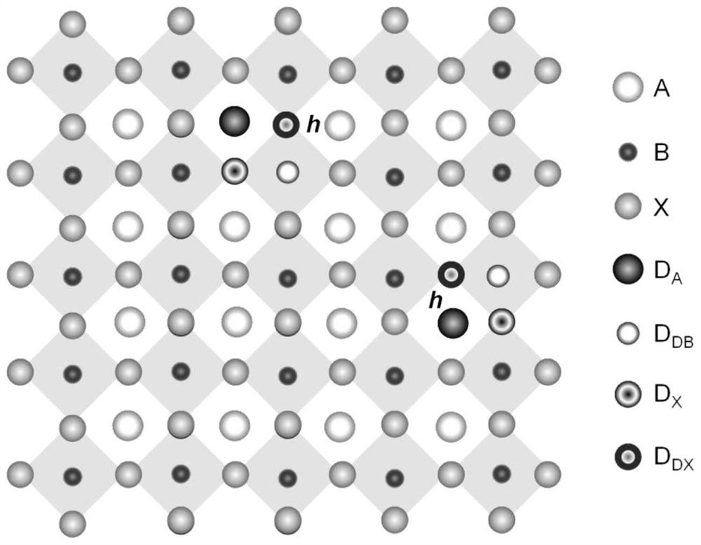
[0026] A P-type doped halide perovskite semiconductor, such as figure 1 As shown, the semiconductor is manufactured by ABX 3 Type halide perovskite or its derivatives and P-type dopant. Among them, ABX 3 In the A-type halide perovskite or its derivatives, the A position is a positive monovalent cation, the B position is a positive divalent cation, and the X position is a negative monovalent halogen or pseudohalogen anion; the P-type dopant is composed of a positive monovalent cation D A , Positive monovalent cation D DB , Negative monovalent anion D X , halogen or pseudohalogen atom D DX Composition; Positive monovalent cation D A Grown in ABX 3 A site of type halide perovskite or its derivatives, positive monovalent cation D DB Grown in ABX as doping element 3 type halide perovskite or its derivatives at the B site, leading to ABX 3 Type halide perovskite or its derivatives generate X-site vacancies, negative monovalent anions D X Grown in ABX 3 X position of type ...

Embodiment 2

[0037] A method for preparing a P-type doped halide perovskite semiconductor as described in Embodiment 1, comprising:

[0038] Adding D to the precursor of halide perovskite or its derivatives A 、D DB 、D X 、D DX A dopant, using the precursor to prepare a halide perovskite to obtain a P-type doped halide perovskite semiconductor; or,

[0039] Place the halide perovskite or its derivatives in D A 、D DB 、D X 、D DX In the solution or vapor atmosphere of the dopant, by diffusion, a P-type doped halide perovskite semiconductor is obtained; or,

[0040] Adding D to the precursor of halide perovskite or its derivatives A 、D DB 、D X 、D DX One or more of the dopants, the precursor is used to prepare the halide perovskite, and the prepared halide perovskite is placed in the solution or vapor atmosphere of the remaining several dopants, and by diffusion, the obtained P-type doped halide perovskite semiconductors.

[0041] The preparation method of the P-type halide perovskit...

example 1

[0043] Example 1: P-type MAPbI 3 Halide perovskite and its preparation

[0044] Weigh 1mmol of methylamine iodide MAI, 1mmol of lead iodide PbI 2 , to which was added 0.01 mmol of MAI, 0.01 mmol of KI iodide, 0.005 mmol of iodine I 2 , then add 1mL of DMF solvent, stir and dissolve to obtain a P-type doped perovskite precursor solution; weigh 1mmol of MAI, 1mmol of PbI 2 , add 1mL of DMF solvent to it, and configure the reference perovskite precursor solution; take the P-type doped perovskite precursor solution and the reference perovskite precursor solution, and spin-coat on the conductive glass substrate to prepare MAPbI 3 Perovskite film; the work function of the obtained film was tested, and it was found that the MAPbI prepared by using the P-type doped precursor solution 3 The work function of the perovskite film increased by 0.7eV compared with the reference film. The conductivity of the two perovskite films was measured at the same time, and it was found that the con...


PUM


Abstract

The invention belongs to the field of halide perovskite semiconductors, in particular to a P-type doped halide perovskite semiconductor and a preparation method thereof. The semiconductor is produced by ABX 3 Type halide perovskite or its derivatives and P-type dopant; wherein the P-type dopant is composed of positive monovalent cation D A , Positive monovalent cation D DB , Negative monovalent anion D X , halogen or pseudohalogen atom D DX Composition; D A Grown on the A site of perovskite or its derivatives, D DB As a doping element, it grows on the B site of perovskite or its derivatives, and causes perovskite or its derivatives to generate X site vacancies, D X Occupying the X site of perovskite or its derivatives, D DX As a doping element occupying the doping element D DB leads to a vacancy in X and leads to ABX 3 Type halide perovskite or its derivatives generate holes to form P-type doped halide perovskite semiconductor. The invention breaks through the short board of the P-type lattice doped halide perovskite semiconductor, and facilitates the further development of halide perovskite semiconductor electronic / optoelectronic devices.

Description

technical field [0001] The invention belongs to the field of halide perovskite semiconductors, and more specifically relates to a P-type doped halide perovskite semiconductor and a preparation method thereof. Background technique [0002] Materials, energy, and information are the three cornerstones of the progress of human society. The emergence and application of semiconductor materials have greatly promoted the development of human society. On the one hand, semiconductor materials are widely used in the information field, such as chips and display panels that rely on transistors, and various detectors that rely on semiconductors; on the other hand, semiconductor materials can also be used in the energy field represented by solar cells. The development and application of solar cell technology has an extremely important strategic position for the acquisition of clean and sustainable energy. Since the emergence of semiconductor technology, silicon semiconductor materials ar...

Claims


Application Information

Patent Timeline
Patent Type & Authority Patents(China)
IPC IPC(8): H01L51/42H01L51/46H01L51/50H01L51/54
CPCH10K85/00H10K30/00H10K50/00Y02E10/549
Inventor 韩宏伟梅安意
Owner HUAZHONG UNIV OF SCI & TECH
Why Eureka
Try Eureka