LED epitaxial structure and application thereof, light-emitting diode comprising LED epitaxial structure and preparation method of LED epitaxial structure

A technology of light-emitting diodes and epitaxial structures, which is applied in the direction of electrical components, circuits, semiconductor devices, etc., can solve the problems of blocking photon overflow and low brightness, and achieve the effects of increasing horizontal expansion ability, improving crystal quality, and improving brightness

Active Publication Date: 2021-10-29
HUAIAN AUCKSUN OPTOELECTRONICS TECHNOLOGY CO LTD
View PDF6 Cites 0 Cited by
  • Summary
  • Abstract
  • Description
  • Claims
  • Application Information

AI Technical Summary

Problems solved by technology

[0005]Although the p-type contact layer and the electrode in the above two patents can form a good ohmic contact, the p-type contact layer will block the overflow of photons, resulting in uneven brightness. Low

Method used


Image

  • LED epitaxial structure and application thereof, light-emitting diode comprising LED epitaxial structure and preparation method of LED epitaxial structure
  • LED epitaxial structure and application thereof, light-emitting diode comprising LED epitaxial structure and preparation method of LED epitaxial structure
  • LED epitaxial structure and application thereof, light-emitting diode comprising LED epitaxial structure and preparation method of LED epitaxial structure

Examples


Embodiment approach 1

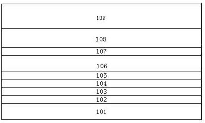
[0034] This implementation mode provides an LED epitaxial structure, such as figure 1As shown, it includes a patterned sapphire substrate 101, an AlN nucleation layer 102, a buffer layer 103, an undoped GaN layer 104, a Si-doped n-type GaN layer 105, a multi-quantum well light-emitting layer 106, and An electron blocking layer 107 , a Mg-doped p-type GaN layer 108 and a p-type contact layer 109 .

[0035] The material of the electron blocking layer 107 is p-type Al doped with Mg 0.2 In 0.1 Ga 0.7 N layer, thickness is 30nm; Mg doping concentration is 2E+20Atom / cm 3 .

[0036] The material of the Mg-doped p-type GaN layer 108 is a Mg-doped p-type Al0.1Ga0.9N layer with a thickness of 30nm; the Mg doping concentration is 6E+19Atom / cm 3 .

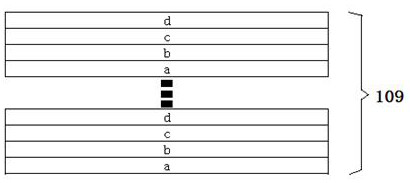
[0037] Such as figure 2 As shown, the above-mentioned p-type contact layer 109 is four p-type GaN / p-type In layers grown periodically from bottom to top 0.2 Ga 0.8 N / p type Al 0.2 In 0.2 Ga 0.6 N / MgN superlattice layer, the thickn...

Embodiment approach 2

[0054] This embodiment is roughly the same as Embodiment 1, except that the p-type contact layer 109 in this embodiment is four p-type GaN / p-type In layers grown periodically from bottom to top. 0.1 Ga 0.9 N / p type Al 0.2 In 0.1 Ga 0.7 N / MgN superlattice layer, wherein the thickness of p-type GaN layer a is 2nm; p-type In 0.1 Ga 0.9 The thickness of N layer b is 2nm; p-type Al 0.2 In 0.1 Ga 0.7 The thickness of the N layer c is 2 nm; the thickness of the MgN layer d is 1 nm.

[0055] Apart from this, this embodiment is completely the same as Embodiment 1, and details are not repeated here.

Embodiment approach 3

[0057] This embodiment is roughly the same as Embodiment 1, except that the p-type contact layer 109 in this embodiment is four p-type GaN / p-type In layers grown periodically from bottom to top. 0.3 Ga 0.7 N / p type Al 0.2 In 0.3 Ga 0.5 N / MgN superlattice layer, wherein the thickness of p-type GaN layer a is 2nm; p-type In 0.3 Ga 0.7 The thickness of N layer b is 2nm; p-type Al 0.2 In 0.3 Ga 0.5 The thickness of the N layer c is 2 nm; the thickness of the MgN layer d is 1 nm.

[0058] Apart from this, this embodiment is completely the same as Embodiment 1, and details are not repeated here.


PUM

PropertyMeasurementUnit
Thicknessaaaaaaaaaa
Thicknessaaaaaaaaaa
Thicknessaaaaaaaaaa

Abstract

The invention relates to the field of semiconductor illumination, and discloses an LED epitaxial structure and application thereof, a light-emitting diode comprising the LED epitaxial structure and a preparation method of the LED epitaxial structure, and the LED epitaxial structure comprises a substrate, a buffer layer, an n type GaN layer, a multi-quantum well light-emitting layer, a p -type GaN layer and a p type contact layer which are sequentially arranged from bottom to top; the p type contact layer is sequentially provided with a p type GaN layer, a p type InaGa1-aN layer, a p type AlbIncGa1-b-cN layer and an MgN layer from bottom to top, wherein a is larger than 0 and is less tha 1, 1-a is larger than 0 and is less than 1, b is larger than 0 and is less than 1, c is larger than 0 and is less than 1, and 1-b-c is larger than 0 and is less than 1. According to the invention, the p type contact layer in the LED epitaxial structure can improve the ohmic contact effect with the p electrode, reduce the ohmic contact resistance, and facilitate the photon overflow of the multi-quantum well light-emitting layer, thereby improving the photoelectric characteristics of a light-emitting diode; current diffusion is facilitated, and the antistatic capability of the light-emitting diode is improved.

Description

technical field [0001] The invention relates to the field of semiconductor lighting, in particular to an LED epitaxial structure and its application, a light emitting diode containing the structure and a preparation method thereof. Background technique [0002] Because light-emitting diodes have the advantages of energy saving and environmental protection, smart design, long life, etc., they have been developed rapidly in recent years. In particular, the success of III-V nitride semiconductor LED technology in the field of blue light has directly promoted the entry of LED lighting into thousands of households. The current mainstream GaN-based light-emitting diode chip structure is: patterned sapphire substrate, AlN nucleation layer, buffer layer, non-doped GaN layer, Si-doped n-type GaN layer, multiple quantum well light-emitting layer, electron blocking layer, Mg-doped p-type GaN layer. In order to facilitate wiring and external forward voltage to make the device emit lig...

Claims


Application Information

Patent Timeline
IPC IPC(8): H01L33/04H01L33/06H01L33/14H01L33/36H01L33/40H01L33/00
CPCH01L33/36H01L33/40H01L33/04H01L33/06H01L33/14H01L33/007H01L2933/0016
Inventor 王明军郭园展望芦玲
Owner HUAIAN AUCKSUN OPTOELECTRONICS TECHNOLOGY CO LTD
Why Eureka
Try Eureka