

Electroluminescent diode device and preparation method thereof, and display device
A luminescence and diode technology, applied in the field of electronic display, can solve the problems of quantum dot charging, hole and electron number imbalance, Auger recombination, etc., and achieve the effect of increasing potential barrier, reducing electron injection, and dense packing
- Summary
- Abstract
- Description
- Claims
- Application Information
AI Technical Summary
Problems solved by technology
Method used
Image

Examples
preparation example Construction
[0057] An embodiment of the present invention also provides a method for preparing an electroluminescent diode device, the electroluminescent diode device prepared by the method can be the aforementioned electroluminescent diode device, and thus, the method can have the aforementioned electroluminescent diode device. All the features and advantages of electroluminescent diode devices. The method includes the following steps.
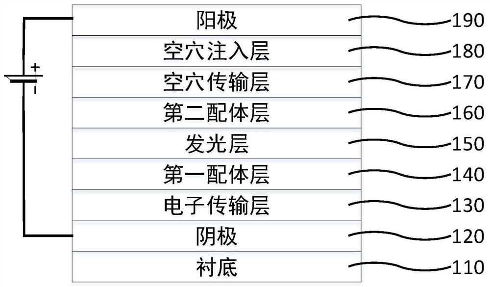
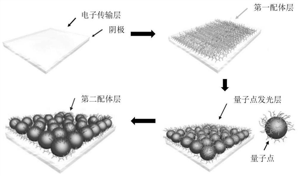
[0058] forming a cathode, an electron transport layer, a first ligand layer, a light emitting layer, a second ligand layer, a hole transport layer and an anode in sequence on the substrate; or
[0059] forming an anode, a hole transport layer, a second ligand layer, a light-emitting layer, a first ligand layer, an electron transport layer and a cathode in sequence on the substrate;
[0060] Wherein, the light-emitting layer is a quantum dot light-emitting layer, which includes quantum dots and surface ligands combined with the quantum dots.
[0061] Pr...
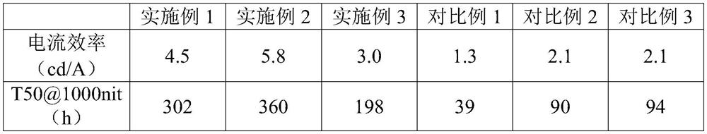
Embodiment 1
[0084] (1) Prepare the ITO cathode on the glass substrate by evaporation; spin the zinc oxide ink on the ITO cathode by spin coating on the ITO cathode, vacuum dry the film and anneal at 120°C for 15 minutes to form electrons The transport layer has a thickness of 45 nm.
[0085] (2) N,N,N',N'-tetrakis(N-(2-aminoethyl)propionamido)ethylenediamine was dissolved in methanol, and spin-coated on the electron transport layer by spin coating During the spin coating process, the rotational speed was 3000 rpm, and the spin coating time was 30 s, and then the excess amide compounds were rinsed off with methanol to form the first ligand layer.
[0086] (3) Prepare a light-emitting layer on the first ligand layer, spin-coat the CdZnS (core material) / ZnS (shell material) quantum dot ink on the first ligand layer, and dry it in a vacuum to form a film and then anneal it at 100° C. for 10 minutes to form a The light-emitting layer has a thickness of 20 nm. The surface ligand of the quantu...
Embodiment 2
[0093] (1) Prepare the ITO cathode on the glass substrate by evaporation; spin the zinc oxide ink on the ITO cathode by spin coating on the ITO cathode, vacuum dry the film and anneal at 120°C for 15 minutes to form electrons The transport layer has a thickness of 45 nm.
[0094] (2) N,N,N',N'-tetrakis(N-(2-aminoethyl)propionamido)ethylenediamine was dissolved in methanol, and spin-coated on the electron transport layer by spin coating During the spin coating process, the rotational speed was 3000 rpm, and the spin coating time was 30 s, and then the excess amide compounds were rinsed off with methanol to form the first ligand layer.
[0095] (3) Prepare a light-emitting layer on the first ligand layer, spin-coat the CdZnS (core material) / ZnS (shell material) quantum dot ink on the first ligand layer, and dry it in a vacuum to form a film and then anneal it at 100° C. for 10 minutes to form a The light-emitting layer has a thickness of 20 nm. The surface ligand of the quantu...
PUM
 Abstract
Description
Claims
Application Information