Compact maskless photoetching system and exposure method thereof
A maskless lithography, compact technology, applied in the field of projection lithography technology, can solve the problems of large size of optical components, reduction of system volume, increase of system cost, etc., to improve lithography efficiency, simplify optical path structure, utilize rate-boosting effect
- Summary
- Abstract
- Description
- Claims
- Application Information
AI Technical Summary
Problems solved by technology
Method used
Image
Examples
Embodiment Construction
[0037] In order to facilitate those skilled in the art to understand the technical content of the present invention, the content of the present invention will be further explained below in conjunction with the accompanying drawings.
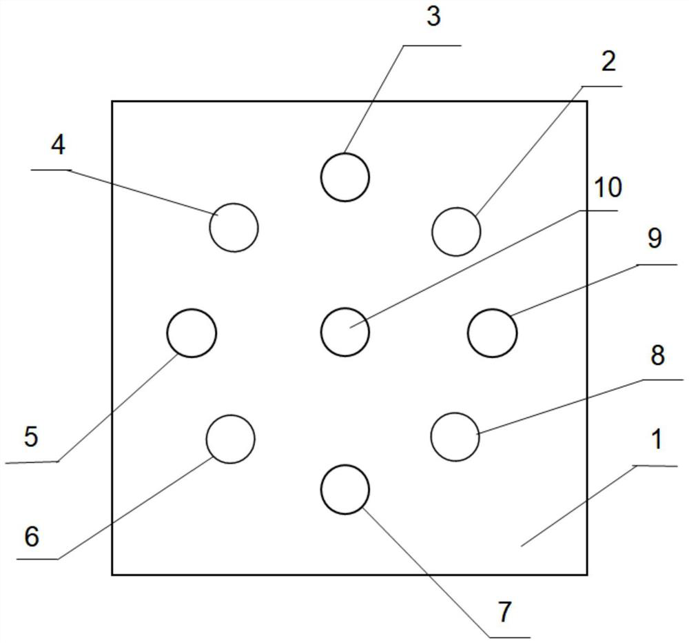
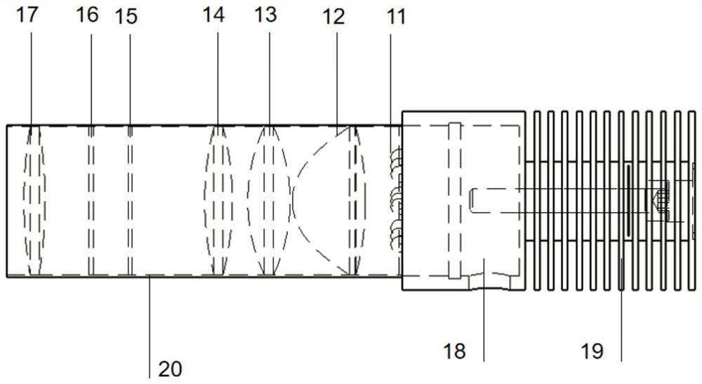
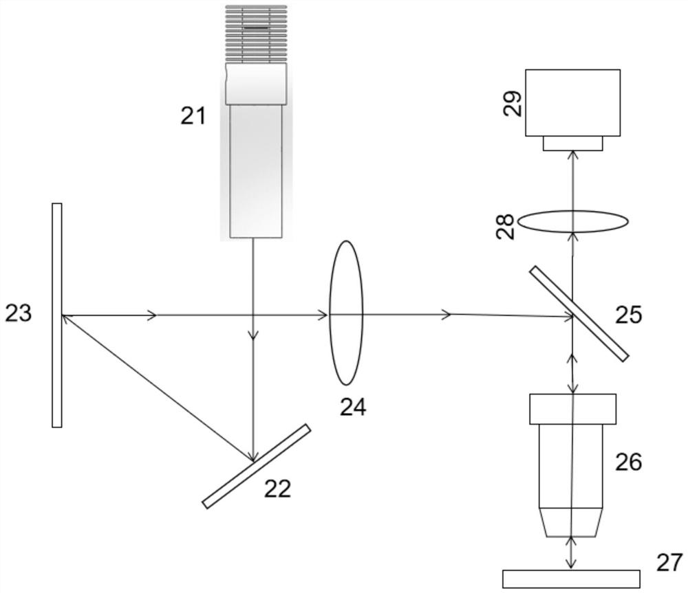
[0038] DMD-based visual maskless lithography generally uses light with wavelengths of 436nm, 405nm, and 365nm as the lithography light source, taking 405nm as an example. The 650nm red light is selected as the illumination and alignment light source, because it does not interact with the photoresist, and the camera can collect the image of the red light passing through the DMD and the subsequent optical path on the photoresist. Since 405nm purple light is the exposure light source, higher light intensity is required, while red light only serves as an illumination alignment, and the optical power does not need to be too high, so multiple purple light LEDs and one red light LED are integrated on one panel .
[0039] The number of specific purple L...
PUM
 Abstract
Description
Claims
Application Information


