

Chemical mechanical polishing solution
A chemical mechanical and polishing liquid technology, which is applied in the fields of polishing compositions containing abrasives, electrical components, semiconductor/solid-state devices, etc., can solve the problem that the polishing rate and planarization efficiency of dielectric materials cannot be taken into account at the same time, and achieve flatness The effects of high chemical efficiency, high polishing rate, and simplified steps
- Summary
- Abstract
- Description
- Claims
- Application Information
AI Technical Summary
Problems solved by technology
Method used
Image

Examples
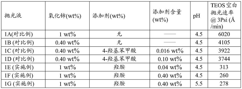
Embodiment 1
[0022] In the present embodiment, the reference example contains 1wt% sol-type cerium oxide, and other embodiments and comparative examples then add or reduce a certain amount of compound and cerium oxide (see Table 1) on the basis of the reference example, and use ammoniacal liquor (NH4OH ) or nitric acid (HNO3) to adjust the pH to 4.5, and make up the mass percentage to 100% with water.
[0023] Polishing method: Mirra polishing machine is used to perform polishing test on TEOS (silicon oxide) blank wafer (hereinafter referred to as "TEOS blank"). The corresponding polishing conditions include: IC1010 polishing pad, polishing disc (Platten) and polishing head (Carrier) speed They are 93rpm and 87rpm respectively, the pressure is 3psi, the flow rate of polishing fluid is 150mL / min, and the polishing time is 60 seconds. The TEOS film thickness is measured with a NanoSpec non-metallic film thickness measuring instrument (NanoSpec6100-300). Starting at 3mm from the edge of the ...
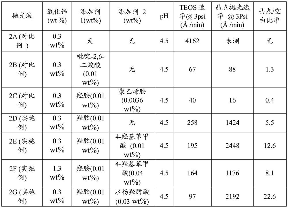
Embodiment 2
[0030] In the present embodiment, the reference example contains 0.3wt% sol-type cerium oxide, and other embodiments and comparative examples add a certain amount of compound or cerium oxide (see Table 2) on the basis of the reference example, and use ammonia water (NH 4 OH) or nitric acid (HNO 3 ) to adjust the pH to 4.5, and make up the mass percentage to 100% with water.
[0031] Polishing method: Mirra polishing machine is used for polishing to test TEOS blank and patterned wafers. The corresponding polishing conditions include: IC1010 polishing pad, polishing disc (Platten) and polishing head (Carrier) with speeds of 93rpm and 87rpm respectively , pressure 3psi, polishing fluid flow rate 150mL / min. The TEOS film thickness was measured with a NanoSpec film thickness measurement system (NanoSpec6100-300, Shanghai Nanospec Technology Corporation). Starting at 3mm from the edge of the wafer, measure 49 points at equal intervals on the diameter line. The polishing rate is a...
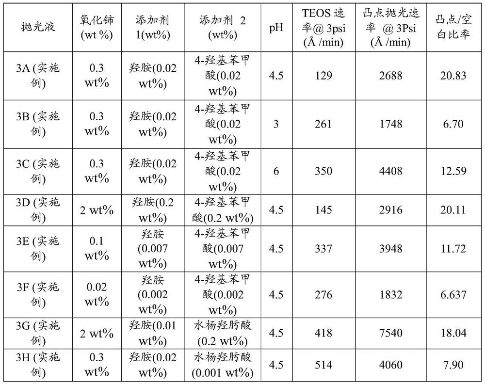
Embodiment 3
[0040] In the present embodiment, the reference example contains 0.3wt% sol-type cerium oxide, and other embodiments then add a certain amount of compound and change the content of the sol-type cerium oxide on the basis of the reference example (see Table 2), and use ammonia ( NH 4 OH) or nitric acid (HNO 3 ) to adjust the pH to 4.5, and make up the mass percentage to 100% with water.
[0041] Polishing method: Mirra polishing machine is used for polishing to test TEOS blank and patterned wafers. The corresponding polishing conditions include: IC1010 polishing pad, polishing disc (Platten) and polishing head (Carrier) with speeds of 93rpm and 87rpm respectively , pressure 3psi, polishing fluid flow rate 150mL / min. The TEOS film thickness was measured with a NanoSpec film thickness measuring system (NanoSpec6100-300, Shanghai Nanospec Technology Corporation). Starting at 3mm from the edge of the wafer, measure 49 points at equal intervals on the diameter line. The polishing...
PUM
 Abstract
Description
Claims
Application Information