Semiconductor process equipment
A process equipment and semiconductor technology, applied in semiconductor/solid-state device manufacturing, metal material coating process, vacuum evaporation plating, etc., can solve the problems of difficult detection of film deposition rate, etc., and achieve low detection difficulty, not easy to damage, The effect of simple process
- Summary
- Abstract
- Description
- Claims
- Application Information
AI Technical Summary
Problems solved by technology
Method used
Image

Examples
Embodiment Construction
[0024] In order to make the purpose, technical solution and advantages of the present invention clearer, the technical solution of the present invention will be clearly and completely described below in conjunction with specific embodiments of the present invention and corresponding drawings. Apparently, the described embodiments are only some of the embodiments of the present invention, but not all of them. Based on the embodiments of the present invention, all other embodiments obtained by persons of ordinary skill in the art without making creative efforts belong to the protection scope of the present invention.
[0025] The technical solutions disclosed by various embodiments of the present invention will be described in detail below in conjunction with the accompanying drawings.
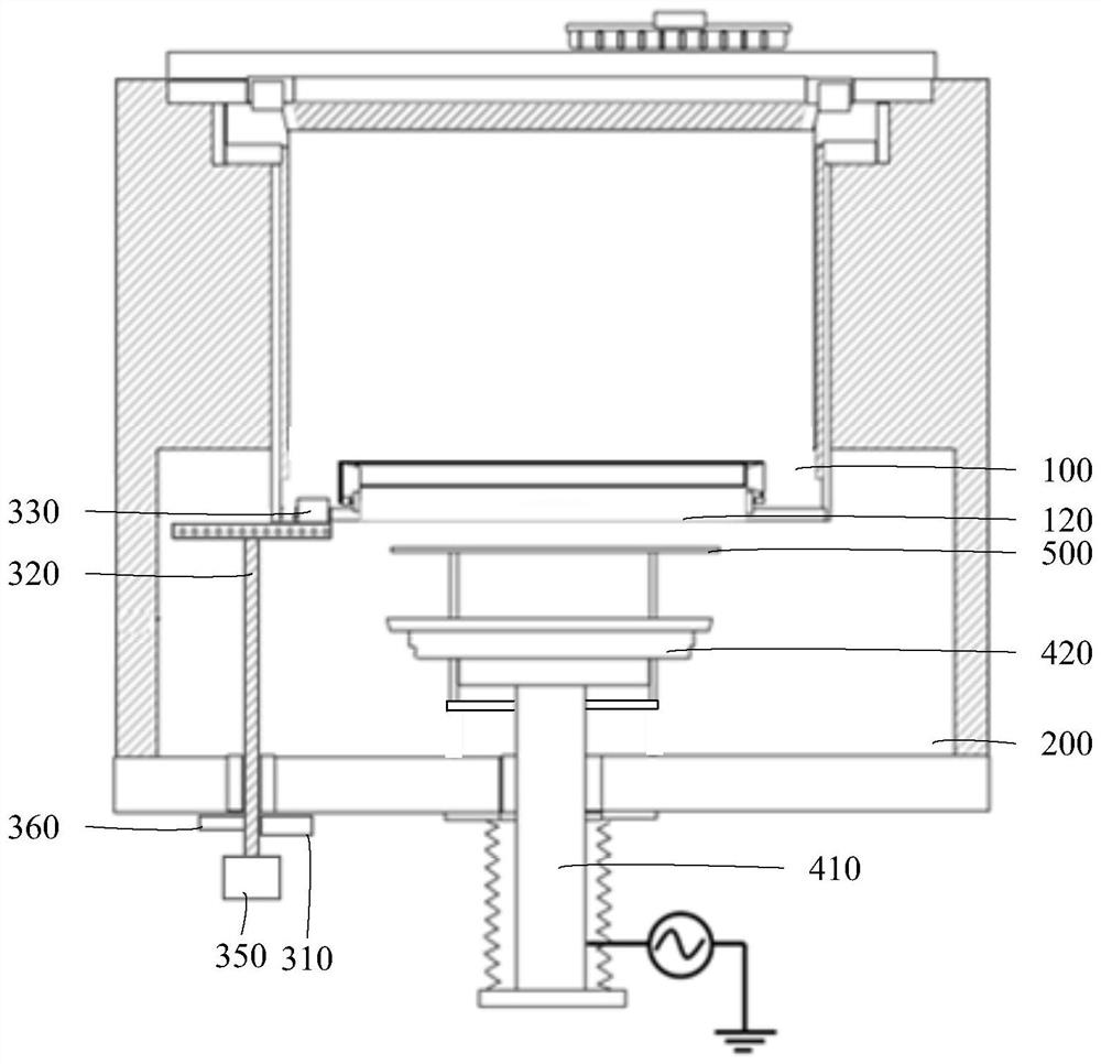
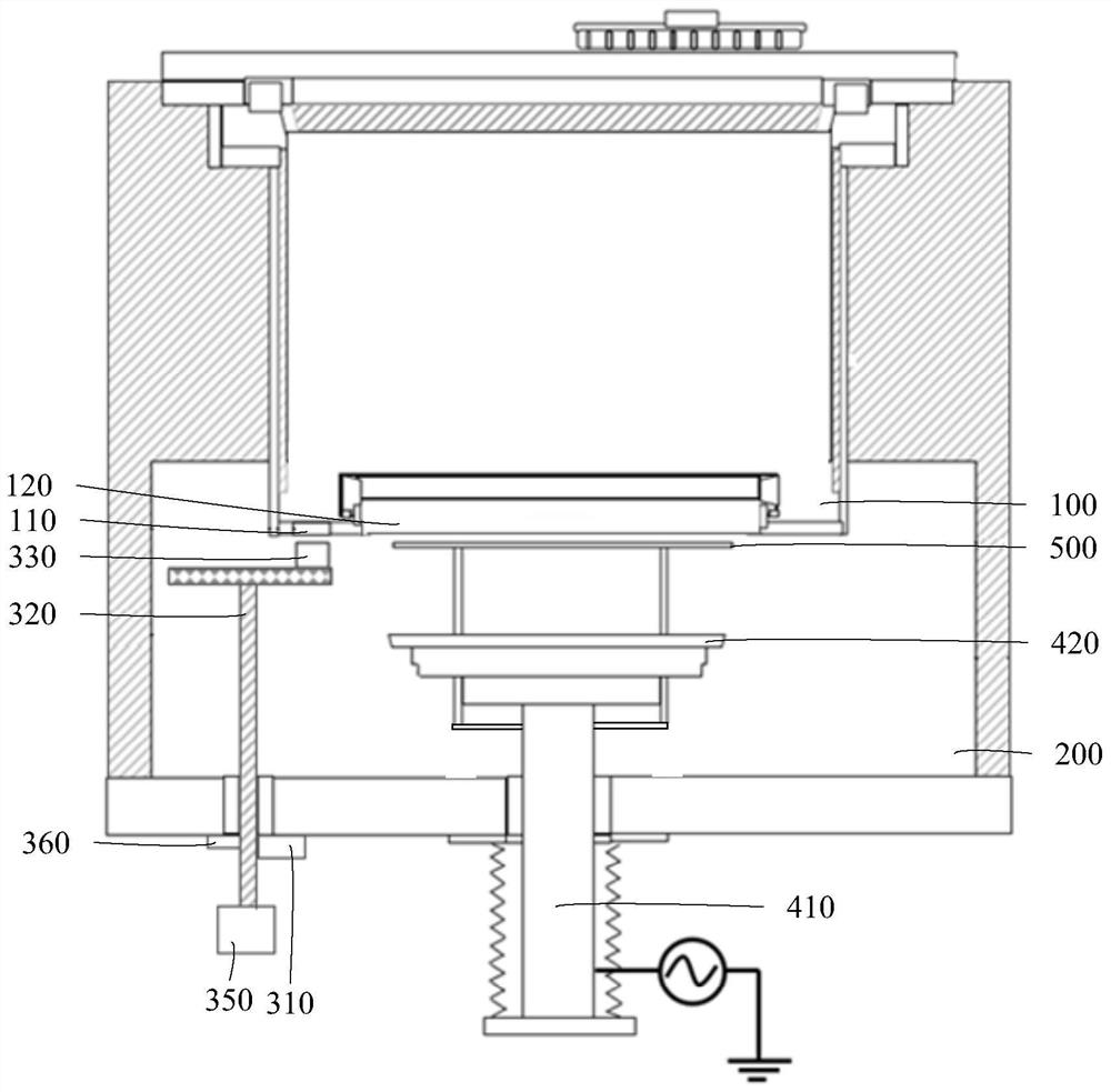
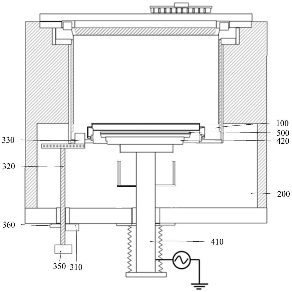
[0026] Such as Figure 1 to Figure 5 As shown, the embodiment of the present invention discloses a semiconductor process equipment, which is used for depositing a thin film for the wafer 500, a...
PUM
 Abstract
Description
Claims
Application Information
 - Generate Ideas
- Intellectual Property
- Life Sciences
- Materials
- Tech Scout
- Unparalleled Data Quality
- Higher Quality Content
- 60% Fewer Hallucinations
Browse by: Latest US Patents, China's latest patents, Technical Efficacy Thesaurus, Application Domain, Technology Topic, Popular Technical Reports.
© 2025 PatSnap. All rights reserved.Legal|Privacy policy|Modern Slavery Act Transparency Statement|Sitemap|About US| Contact US: help@patsnap.com