Piezoresistive miniature electric field sensor, preparation method thereof and electric field sensor

An electric field sensor and piezoresistive technology, which is applied in the fields of electromagnetic field characteristics, electrostatic field measurement, and measurement of the property and force of piezoresistive materials, can solve the problem of high power consumption, achieve low power consumption, realize batch manufacturing and System integration, the effect of reducing manufacturing costs

Pending Publication Date: 2021-07-09
AEROSPACE INFORMATION RES INST CAS
View PDF9 Cites 5 Cited by
  • Summary
  • Abstract
  • Description
  • Claims
  • Application Information

AI Technical Summary

Problems solved by technology

Most of the proposed MEMS electric field sensors use an external driving voltage to drive the displacement of the driving structure, and then realize the measurement of the electric field to be measured based on the principle of charge induction, which is limited by the working principle and also brings high power consumption. shortcoming

Method used


Image

  • Piezoresistive miniature electric field sensor, preparation method thereof and electric field sensor
  • Piezoresistive miniature electric field sensor, preparation method thereof and electric field sensor
  • Piezoresistive miniature electric field sensor, preparation method thereof and electric field sensor

Examples


preparation example Construction

[0058] The invention also discloses a preparation method of a piezoresistive miniature electric field sensor, comprising:

[0059] Step 1: Write a pattern on the photoresist layer 704 above the device layer 701 on the top of the SOI wafer. The pattern includes: the shape pattern of the vibration film 1, the shape pattern of the support beam 2, the shape pattern of the piezoresistive pickup element 3 and the anchor region 4 shape pattern;

[0060] Wherein, at least one end of the piezoresistive vibration pickup element 3 is connected to the anchor region 4;

[0061] Wherein, the vibrating membrane 1 is connected with the piezoresistive vibration pickup element 3 through the support beam 2;

[0062] Step 2: Etch the device layer 701 on the top of the SOI wafer according to the pattern described in step 1, form the vibration film 1, the support beam 2, the piezoresistive pickup element 3 and the anchor region 4, and remove the photoresist layer 704;

[0063] Step 3: Etching a w...

Embodiment 1

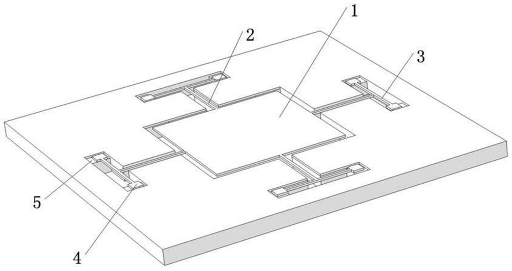
[0081] Such as figure 1 As shown, piezoresistive miniature electric field sensors include:

[0082] The vibration film 1 is connected to the piezoresistive pickup element 3 through the support beam 2 , and the piezoresistive pickup element 3 is fixed on the top of the substrate 5 through the anchor region 4 .

[0083] The vibrating membrane 1 can be a square membrane structure, and the square membrane structure has no through holes.

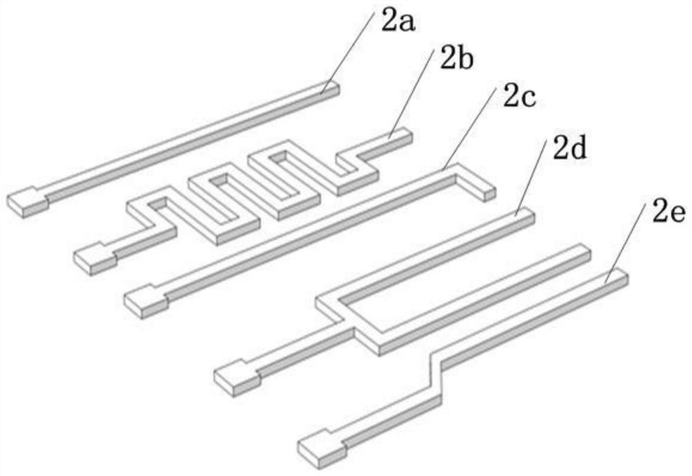
[0084] Such as figure 2 As shown, the shape of the support beam 2 can be a straight beam 2a, a serpentine beam 2b, an L-shaped beam 2c, a U-shaped beam 2d or an irregular beam 2e, etc. The support beam 2 in this embodiment adopts a straight beam 2a, One end of the support beam 2 is set at the midpoint of the piezoresistive pickup element 3 , and the other end is set at the midpoint of the side of the vibrating membrane 1 .

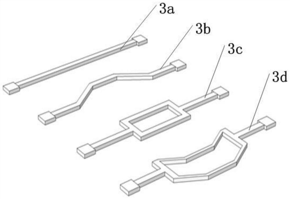
[0085] The piezoresistive vibration pickup element 3 in this embodiment adopts a straight beam structure 3 a, and both ...

Embodiment 2

[0087] Such as Figure 4 As shown, the difference between the piezoresistive miniature electric field sensor in this embodiment and Embodiment 1 is that the piezoresistive vibration pickup element 3 adopts a tuning fork beam structure 3c.

[0088] In one embodiment of the present invention, a preparation method of a piezoresistive miniature electric field sensor is also disclosed;

[0089] Such as Figure 5 shown, including the following steps:

[0090] S1: Spin-coat a photoresist layer 704 on the device layer 701 of the SOI wafer as a mask material, and use a mask plate to perform photolithography to form a Figure 5 The structural shape shown in Figure A;

[0091] S2: The sensor vibration film 1, the support beam 2, the piezoresistive pickup element 3 and the anchor region 4 are etched on the device layer 701 by using the DRIE process, and the photoresist layer 704 is removed to form a Figure 5 The structural shape shown in Figure B;

[0092] S3: Etch a window on the s...


PUM


Abstract

The invention discloses a piezoresistive miniature electric field sensor, a preparation method thereof and an electric field sensor. The piezoresistive miniature electric field sensor comprises a substrate; an anchor region disposed at the top of the substrate; a piezoresistive vibration pick-up element connected with the anchor area and used for converting the electric field intensity into resistance value change; a vibration film which is suspended above the substrate, is connected with the piezoresistive vibration pick-up element through a supporting beam and is used for sensing the change of an electric field. The vibration film generates displacement under the action of electric field force, so that the resistance value of the piezoresistive vibration pickup structure is changed. The piezoresistive miniature electric field sensor disclosed by the invention does not need to additionally introduce a driving voltage, has the characteristics of low power consumption and capability of realizing alternating-current and direct-current broadband electric field measurement, signals obtained by piezoresistive detection are stronger, the signal-to-noise ratio is high, meanwhile, the size is small, the structure is simple, and batch manufacturing and system integration are facilitated.

Description

technical field [0001] The invention relates to the fields of sensors and micro-electromechanical systems, in particular to a piezoresistive miniature electric field sensor, a preparation method thereof, and an electric field sensor. Background technique [0002] The electric field sensor based on microelectromechanical system (MEMS) is a device used to measure electric field strength, and it is widely used in various fields such as climate and meteorology, power grid, petrochemical industry, aerospace and so on. When electric field sensors form a wireless sensor network for power grid monitoring, the energy consumption and volume of sensor nodes must be considered. [0003] With the development of MEMS technology, compared with traditional electric field sensors, electric field sensors based on MEMS technology are smaller in size, easier to manufacture and integrate. Most of the proposed MEMS electric field sensors use an external driving voltage to drive the displacement ...

Claims


Application Information

Patent Timeline
Patent Type & Authority Applications(China)
IPC IPC(8): G01R29/12G01R29/08G01L1/18
CPCG01R29/12G01R29/0878G01L1/18
Inventor 彭春荣李嘉晨郑凤杰毋正伟任仁吕曜
Owner AEROSPACE INFORMATION RES INST CAS
Why Eureka
Try Eureka