On-chip light source, preparation method of on-chip light source, and optoelectronic device

A light source and optical array technology, applied in electrical components, semiconductor devices, circuits, etc., can solve problems such as weak luminous intensity, low luminous efficiency, slow response speed, etc., and achieve increased luminous intensity, enhanced Purcell effect, and compact structure Effect

Active Publication Date: 2022-02-25
NAT INNOVATION INST OF DEFENSE TECH PLA ACAD OF MILITARY SCI
View PDF0 Cites 0 Cited by
  • Summary
  • Abstract
  • Description
  • Claims
  • Application Information

AI Technical Summary

Problems solved by technology

[0004] The invention provides an on-chip light source, a preparation method of an on-chip light source and an optoelectronic device, which are used to solve the defects of low luminous efficiency, slow response speed and weak luminous intensity of optically integrated light-emitting devices in the prior art

Method used


Image

  • On-chip light source, preparation method of on-chip light source, and optoelectronic device
  • On-chip light source, preparation method of on-chip light source, and optoelectronic device
  • On-chip light source, preparation method of on-chip light source, and optoelectronic device

Examples


Embodiment Construction

[0042] In order to make the purpose, technical solutions and advantages of the present invention clearer, the technical solutions in the present invention will be clearly and completely described below in conjunction with the accompanying drawings in the present invention. Obviously, the described embodiments are part of the embodiments of the present invention , but not all examples. Based on the embodiments of the present invention, all other embodiments obtained by persons of ordinary skill in the art without creative efforts fall within the protection scope of the present invention.

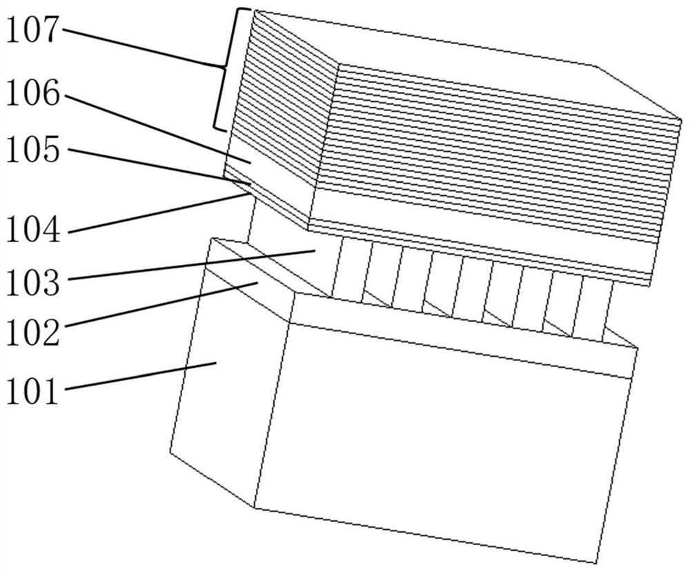
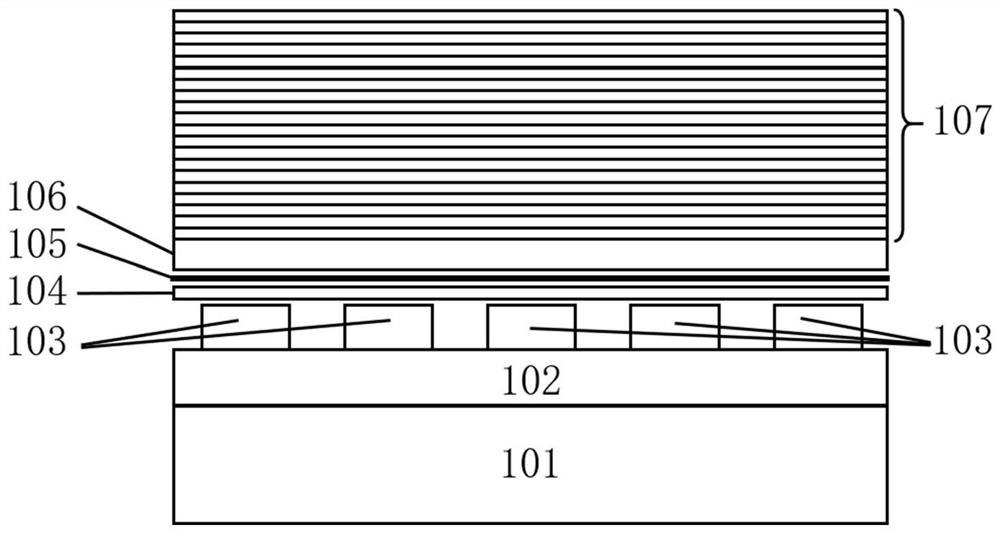
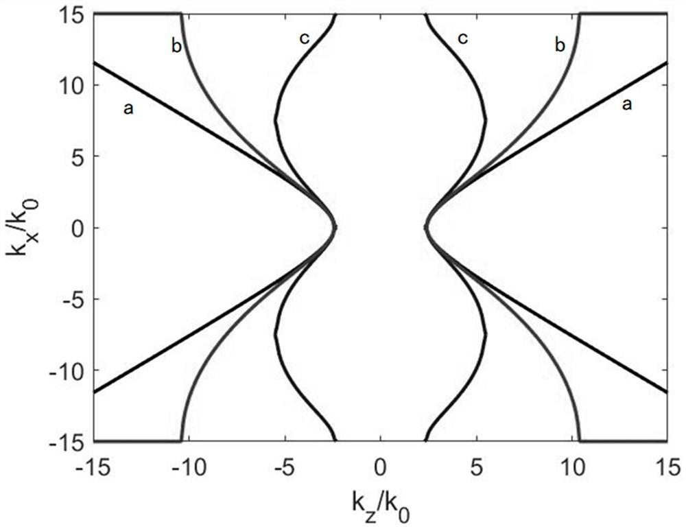
[0043] At present, silicon-based optoelectronics will enter the field of optical communication links on a smaller scale, that is, optical chip-to-optical chip or inside an optical chip. However, the indirect bandgap of silicon, which has an indirect bandgap, leads to low radiation efficiency and is not suitable for making monolithic light sources. In fact, light sources often require optical...


PUM

PropertyMeasurementUnit
thicknessaaaaaaaaaa
thicknessaaaaaaaaaa
thicknessaaaaaaaaaa

Abstract

The invention provides an on-chip light source, a preparation method of an on-chip light source and an optoelectronic device. An insulating layer is formed on a substrate, an optical array layer is formed on the insulating layer, an isolation layer is formed on the optical array layer, and a two-dimensional optical array layer is formed on the isolation layer. The material layer forms a medium layer on the two-dimensional material layer, and forms a hyperbolic metamaterial layer on the medium layer. Wherein, when the resonance peak of the photon mode of the optical array layer is equal to the wavelength of the exciton peak of the two-dimensional material layer, the luminous intensity of the two-dimensional material layer will be enhanced. In addition, the surface plasmons of the hyperbolic metamaterial layer will have a strong coupling with the two-dimensional material layer, further enhancing the Purcell effect. The present invention utilizes hyperbolic metamaterials to enhance the Purcell effect of two-dimensional materials, which can not only significantly improve the luminous intensity of the on-chip light source, but also achieve high luminous efficiency and fast response speed, small size, compact structure, and easy high-density integration And have good CMOS integration process compatibility.

Description

technical field [0001] The invention relates to the technical field of optoelectronic devices and semiconductor manufacturing, in particular to an on-chip light source, a preparation method of the on-chip light source and an optoelectronic device. Background technique [0002] Driven by the era of next-generation supercomputers and big data, silicon-based optoelectronics, with its small size, low power consumption, ultra-large bandwidth, and ultra-fast response speed, has become a leading technology to solve the explosive growth of massive data transmission requirements in optical communication systems . [0003] At present, silicon-based optoelectronics will enter the field of optical communication links on a smaller scale, that is, optical chip-to-optical chip or inside an optical chip. However, the indirect bandgap of silicon, which has an indirect bandgap, leads to low radiation efficiency and is not suitable for making monolithic light sources. In fact, light sources ...

Claims


Application Information

Patent Timeline
Patent Type & Authority Patents(China)
IPC IPC(8): H01L33/20H01L33/18H01L33/16H01L33/44
CPCH01L33/20H01L33/18H01L33/16H01L33/44
Inventor 尤洁罗玉昆郑鑫杨杰欧阳昊
Owner NAT INNOVATION INST OF DEFENSE TECH PLA ACAD OF MILITARY SCI
Why Eureka
Try Eureka