Method for preparing graphene nanonet by using patterned substrate imprinting

A technology for patterning substrates and substrates, applied in nanotechnology, photoengraving process of patterned surface, process for producing decorative surface effects, etc., can solve problems affecting electrical and mechanical properties, etc., and achieve low-defect GNM The preparation, preparation process is simple, and the operation is convenient

Pending Publication Date: 2021-07-13
DEZHOU UNIV
View PDF0 Cites 0 Cited by
  • Summary
  • Abstract
  • Description
  • Claims
  • Application Information

AI Technical Summary

Problems solved by technology

It is worth noting that the current chemical etching method is relatively easy to mass-produce GNMs, but this method will introduce a large number of defects in the structure of Gr, thereby affecting its electrical and mechanical properties.

Method used


Image

  • Method for preparing graphene nanonet by using patterned substrate imprinting
  • Method for preparing graphene nanonet by using patterned substrate imprinting
  • Method for preparing graphene nanonet by using patterned substrate imprinting

Examples


Embodiment 1

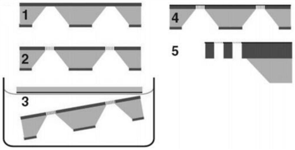
[0076] A method for preparing GNM by embossing a patterned substrate refers to: using a patterned substrate with a higher hardness to emboss a substrate / Gr with a lower hardness, and making the raised pattern of the patterned substrate pass through Through Gr, the preparation of fast, large-area, uniform, low-cost, high-porosity, and low-defect GNMs is realized.

Embodiment 2

[0078] According to a method for preparing GNM by imprinting a patterned substrate according to Embodiment 1, the difference is that:

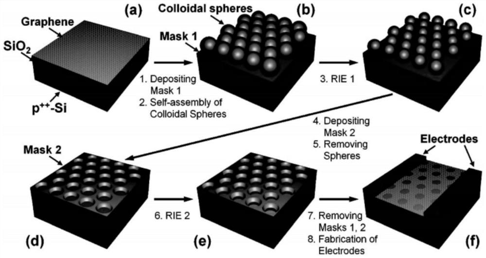
[0079] The method of preparing GNM by imprinting on a patterned substrate is now taking the preparation of GNM by embossing Cu / Gr on a patterned sapphire substrate as an example. The size of the patterned sapphire substrate and Cu / Gr (Cu-based Gr) used are about It is 5mm×5mm. Such as Figure 5 shown, including the following steps:

[0080] (1) Preparation: Prepare the substrate / Gr; Cu / Gr is obtained by directly growing Gr on the Cu substrate by metal organic chemical vapor deposition (MOCVD). The morphology of Cu / Gr is shown in Fig. 7(a), which is single-layer single-crystal (not fully covered).

[0081] (2) Cleaning: Select sapphire with a mode hardness (hardness of 9) greater than Cu as the patterned substrate, and its appearance is as follows Image 6 As shown, the raised pattern is a hemispherical structure arranged periodically, and ...

Embodiment 3

[0090] According to a method for preparing GNM by imprinting a patterned substrate according to Embodiment 2, the difference is that:

[0091] Step (1) refers to: using PMMA to wet transfer Gr to the substrate to prepare the substrate / Gr.

[0092] In step (4), the embossing method includes punching and rolling.

[0093] The number of layers of Gr is single layer or multilayer.

[0094] Periodic raised patterns are prepared by wet etching or dry etching.


PUM


Abstract

The invention relates to a method for preparing a graphene nanonet by using patterned substrate imprinting. The method mainly comprises the steps of substrate / Gr preparation, patterned substrate cleaning, substrate / Gr and patterned substrate assembling, imprinting, demolding and GNM characterization. Compared with the existing GNM preparation method, the preparation method has the advantages that the Gr is penetrated by convex patterns in a patterned substrate in the imprinting process, and rapid, large-area, uniform, low-cost, high-porosity and low-defect GNM preparation can be realized. According to the selection of the patterned substrate, the preparation of GNMs with various patterns and sizes can be realized. In addition, the method adopted by the invention is high in universality, and can be migrated to preparation of nanonets of other two-dimensional materials except Gr, such as MoS2 and BN.

Description

technical field [0001] The invention relates to a method for preparing a graphene nano-network (GNM) by embossing a patterned substrate, which belongs to the field of semiconductor material preparation and processing. Background technique [0002] Since the advent of graphene (Gr), patterned Gr has received extensive attention and research and has applications in various fields such as Gr photonics, plasmonics, and supercapacitors. Many Gr porous materials have thus been born, such as Gr nanomesh (GNM), pleated Gr (CG) and Gr foam (GF), etc. Among them, GNM refers to the formation of high-density nanoscale or subnanoscale hole arrays in one or more layers of Gr. There are mainly two structural parameters in GNM: neck width and periodicity, which are defined as the minimum edge-to-edge distance and center-to-center distance between two adjacent pores in a nanomesh, respectively. This nanoporous structure and its density distribution have a very important influence on the el...

Claims


Application Information

Patent Timeline
Patent Type & Authority Applications(China)
IPC IPC(8): B81C1/00B82Y40/00G03F7/00
CPCB81C1/0046B82Y40/00G03F7/0002
Inventor 贾冉许士才刘汉平刘辉兰乔梅刘国锋
Owner DEZHOU UNIV
Why Eureka
Try Eureka