
Millimeter wave CMOS numerical control attenuator with innovative structure

A digitally controlled attenuator and millimeter wave technology, applied in frequency-independent attenuators, multi-terminal-to-network and other directions, can solve the problems of small attenuation range, high insertion loss and low tuning accuracy of attenuators in the millimeter wave band, and reduce insertion loss. loss, precise gain control, and the effect of achieving gain control

Pending Publication Date: 2021-07-13
SOUTHEAST UNIV
View PDF0 Cites 0 Cited by
  • Summary
  • Abstract
  • Description
  • Claims
  • Application Information

AI Technical Summary

Problems solved by technology

[0004] The purpose of the present invention is to provide a millimeter-wave CMOS numerically controlled attenuator with an innovative structure to solve the technical problems of high insertion loss, low tuning accuracy and small attenuation range of the millimeter-wave frequency band attenuator

Method used


Image

  • Millimeter wave CMOS numerical control attenuator with innovative structure
  • Millimeter wave CMOS numerical control attenuator with innovative structure
  • Millimeter wave CMOS numerical control attenuator with innovative structure

Examples


Embodiment Construction

[0026] In order to better understand the purpose, structure and function of the present invention, a millimeter-wave CMOS digitally controlled attenuator with an innovative structure of the present invention will be further described in detail below in conjunction with the accompanying drawings.

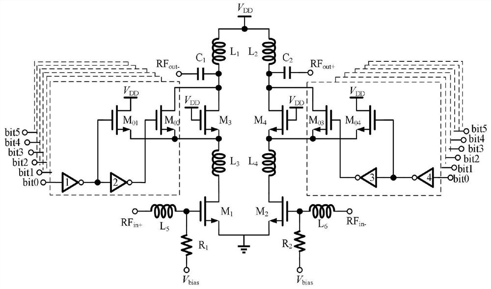
[0027] The central operating frequency of the attenuator circuit in this example is 19GHz. Its overall structure is as figure 1 shown.

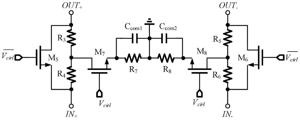
[0028] The invention includes an active gain tuning section and a passive gain tuning section.

[0029] active gain tuning section, that is figure 1 The VGA (Variable Gain Amplifier) ​​module marked in . The gain adjustment part adopts a digital control method, and the equivalent transconductance is changed by changing the number of transistors connected, thereby changing the gain of the circuit. The circuit structure of the active circuit part is as figure 2 shown. RF in+ through the inductance L 5 connected to transistor M 1 gate, V bia...


PUM


Abstract

The invention designs a CMOS (Complementary Metal Oxide Semiconductor) numerical control attenuator applied to a millimeter wave frequency band. In order to simultaneously realize a large attenuation range and small attenuation stepping, the structure adopts a method of combining passive attenuation and active gain adjustment. The passive part provides large attenuation to realize coarse adjustment of the gain, and the active part provides small attenuation to realize fine adjustment of the gain. The control bits of the attenuator are 8 bits, 2 bits of a passive part achieve the attenuation range of 24 dB, and 6 bits of an active part achieve the attenuation range of 7.5 dB. The gain adjustment range which can be realized by the attenuator on the whole is 31.5 dB, and the minimum step is 0.5 dB. By introducing a redundancy state method, high-precision tuning is ensured while a large attenuation range is realized. The millimeter wave frequency band attenuator designed by the invention has the characteristics of large attenuation range, high adjustment precision and small insertion loss. The defects that a traditional active attenuator is small in attenuation range and a passive attenuator is large in insertion loss are overcome.

Description

technical field [0001] The invention belongs to the technical field of electronic communication, and in particular relates to a millimeter-wave CMOS numerically controlled attenuator with an innovative structure. Background technique [0002] With the development of new-generation communication technology, the requirements for seamless coverage and high-speed data transmission of communication systems are getting higher and higher. The millimeter-wave frequency band has abundant spectrum resources, and due to the existence of the atmospheric window, the millimeter-wave frequency band has great potential in high-speed data transmission and short-distance communication. For example, the fifth generation communication (5G) has a part of spectrum distributed in the millimeter wave frequency band. In the millimeter wave frequency band, phased array antennas are often the key equipment. Whether in the receiving channel or the transmitting channel, the attenuation range and atten...

Claims


Application Information

Patent Timeline
IPC IPC(8): H03H11/24
CPCH03H11/24Y02D30/70
Inventor 李芹仲响
Owner SOUTHEAST UNIV
Learn More