Probe test bench for semiconductor processing

A semiconductor and test bench technology, applied in the direction of single semiconductor device testing, measuring electricity, measuring devices, etc., can solve the problems of inconvenient heat dissipation and cooling of test instruments, inconvenient influence of electrical conductivity, complex test equipment, etc.

Inactive Publication Date: 2021-07-16
高必静
View PDF0 Cites 3 Cited by
  • Summary
  • Abstract
  • Description
  • Claims
  • Application Information

AI Technical Summary

Problems solved by technology

[0004] The purpose of the present invention is to solve the problem that the test equipment in the prior art is relatively complicated, and it is not convenient to clamp and fix the semiconductor and adjust the position, and it is not convenient to observe the influence of temperature on the conductivity of the semiconductor, and it is not convenient to dissipate heat and cool down the test instrument , and a probe test bench for semiconductor processing is proposed

Method used


Image

  • Probe test bench for semiconductor processing
  • Probe test bench for semiconductor processing
  • Probe test bench for semiconductor processing

Examples


Embodiment 1

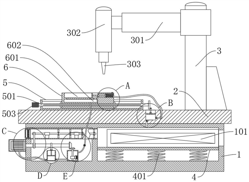
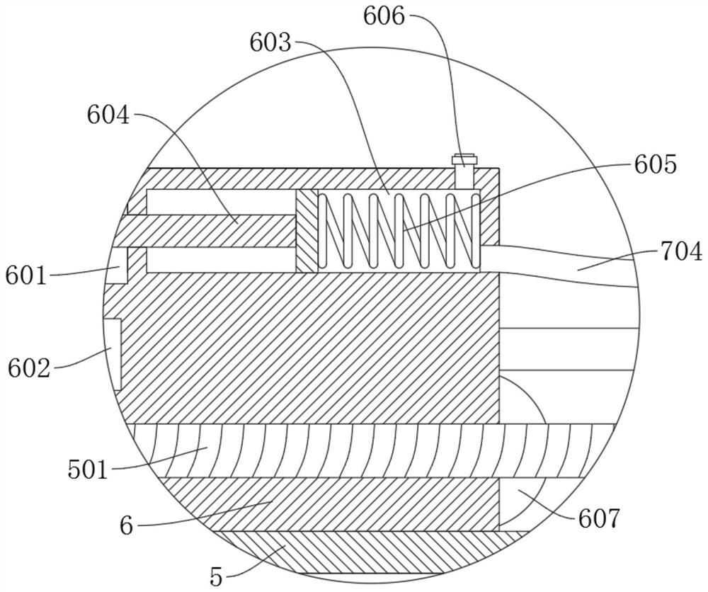
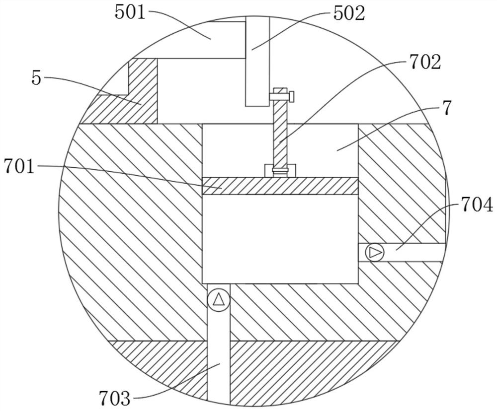
[0038] refer to Figure 1-6 , a probe test bench for semiconductor processing, comprising a base 1, a test platform 2, the test platform 2 is located on the base 1, the test platform 2 is provided with a test mechanism, the base 1 is provided with a test instrument 101, the test mechanism and the test instrument 101 are electrically connected, the test platform 2 is provided with a moving slot 5, and a fixed plate 6 is slidably connected in the moving slot 5. The fixed plate 6 is provided with a placement slot 601, and the fixed plate 6 is provided with a cavity 602. The cavity 602 is located below the placement groove 601, a heat conduction plate is provided between the cavity 602 and the placement groove 601, a threaded rod 501 is rotationally connected in the moving groove 5, and a threaded connection is made between the fixed plate 6 and the threaded rod 501, and the fixed plate 6 is provided with There is a clamping mechanism, the base 1 is connected with a first rotating...

Embodiment 2

[0041] refer to Figure 1-6 , a probe test bench for semiconductor processing, which is basically the same as Embodiment 1, and furthermore, the test mechanism includes a support frame 3, and the support frame 3 is rotatably connected with a first electric telescopic rod 301, and the first electric telescopic rod 301 The telescopic end of the second electric telescopic rod 302 is fixedly connected with the second electric telescopic rod 302, and the telescopic end of the second electric telescopic rod 302 is fixedly connected with the probe part 303, and the probe part 303 matches the fixed plate 6, the first electric telescopic rod 301, the second The setting of the electric telescopic rod 302 is convenient for adjusting the position of the probe part 303 .

Embodiment 3

[0043] refer to Figure 1-6 , a probe test bench for semiconductor processing, which is basically the same as Embodiment 1, furthermore, the first driving mechanism includes a cam 901, and the edge of the side wall of the cam 901 is slidingly connected with a second push rod 122, and the exhaust mechanism Including the second cylinder 12, the second cylinder 12 is slidably connected with the second piston 121, the end of the second push rod 122 away from the cam 901 is fixedly connected with the second piston 121, the second cylinder 12 is provided with a second intake pipe 123, A second exhaust pipe 124 is connected between the second cylinder 12 and the air chamber 13, and a check valve is arranged on the second intake pipe 123 and the second exhaust pipe 124, and the cam 901 drives the second push rod 122 to The piston 121 slides reciprocally in the second cylinder 12, and discharges outside air into the air chamber 13 along the second intake pipe 123 and the second exhaust...


PUM


Abstract

The invention discloses a probe test bench for semiconductor processing, and belongs to the field of semiconductor processing. A probe test bench for semiconductor processing comprises a base and a test platform, the test platform is located on the base, a test mechanism is arranged on the test platform, a test instrument is arranged in the base, the test mechanism is electrically connected with the test instrument, a moving groove is formed in the test platform, a fixing plate is slidably connected in the moving groove, a placement groove is formed in the fixing plate, a cavity is formed in the fixing plate, and the cavity is located below the placement groove. According to the invention, through the arrangement of the cavity, the heat conducting plate, the air pumping and exhausting mechanism, the air bin and the heating mechanism, the influence of temperature change on the performance of the semiconductor is conveniently tested, through the arrangement of the clamping mechanism, the semiconductor is conveniently clamped and fixed, and through the arrangement of a moving groove, a threaded rod and a fixed plate, the position of the semiconductor is conveniently adjusted; and the arrangement of an air pipe, a second rotating shaft and fan blades facilitates heat dissipation and cooling of the test instrument.

Description

technical field [0001] The invention relates to the technical field of semiconductor processing, in particular to a probe test platform for semiconductor processing. Background technique [0002] Semiconductors refer to materials whose conductivity is between conductors and insulators at room temperature. Semiconductors are used in integrated circuits, consumer electronics, communication systems, photovoltaic power generation, lighting, high-power power conversion and other fields. For example, diodes are devices made of semiconductors. , no matter from the perspective of technology or economic development, the importance of semiconductors is very huge. The core units of most electronic products, such as computers, mobile phones or digital recorders, are closely related to semiconductors. , common semiconductor materials include silicon, germanium, gallium arsenide, etc., and silicon is the most influential one in the application of various semiconductor materials. [0003]...

Claims


Application Information

Patent Timeline
Patent Type & Authority Applications(China)
IPC IPC(8): G01R31/26G01R1/04G01R1/02G01R1/14H05K7/20
CPCG01R1/02G01R1/0425G01R1/14G01R31/2601H05K7/20136H05K7/20181
Inventor 不公告发明人
Owner 高必静
Why Eureka
Try Eureka