High-voltage LDMOS device structure with low radiation leakage

A device structure and low-radiation technology, applied in the direction of electric solid-state devices, electrical components, semiconductor devices, etc., can solve the problems of increased device leakage current, reduce off-state loss, avoid leakage, and improve the ability to resist total dose radiation Effect

Active Publication Date: 2021-07-23
UNIV OF ELECTRONICS SCI & TECH OF CHINA
View PDF10 Cites 6 Cited by
  • Summary
  • Abstract
  • Description
  • Claims
  • Application Information

AI Technical Summary

Problems solved by technology

[0003] In order to solve the problem that the device leakage current increases after the total dose of high-voltage LDMOS device is irradiated, the present invention proposes a high-voltage LDMOS device structure with low radiation leakage

Method used


Image

  • High-voltage LDMOS device structure with low radiation leakage
  • High-voltage LDMOS device structure with low radiation leakage
  • High-voltage LDMOS device structure with low radiation leakage

Examples


Embodiment

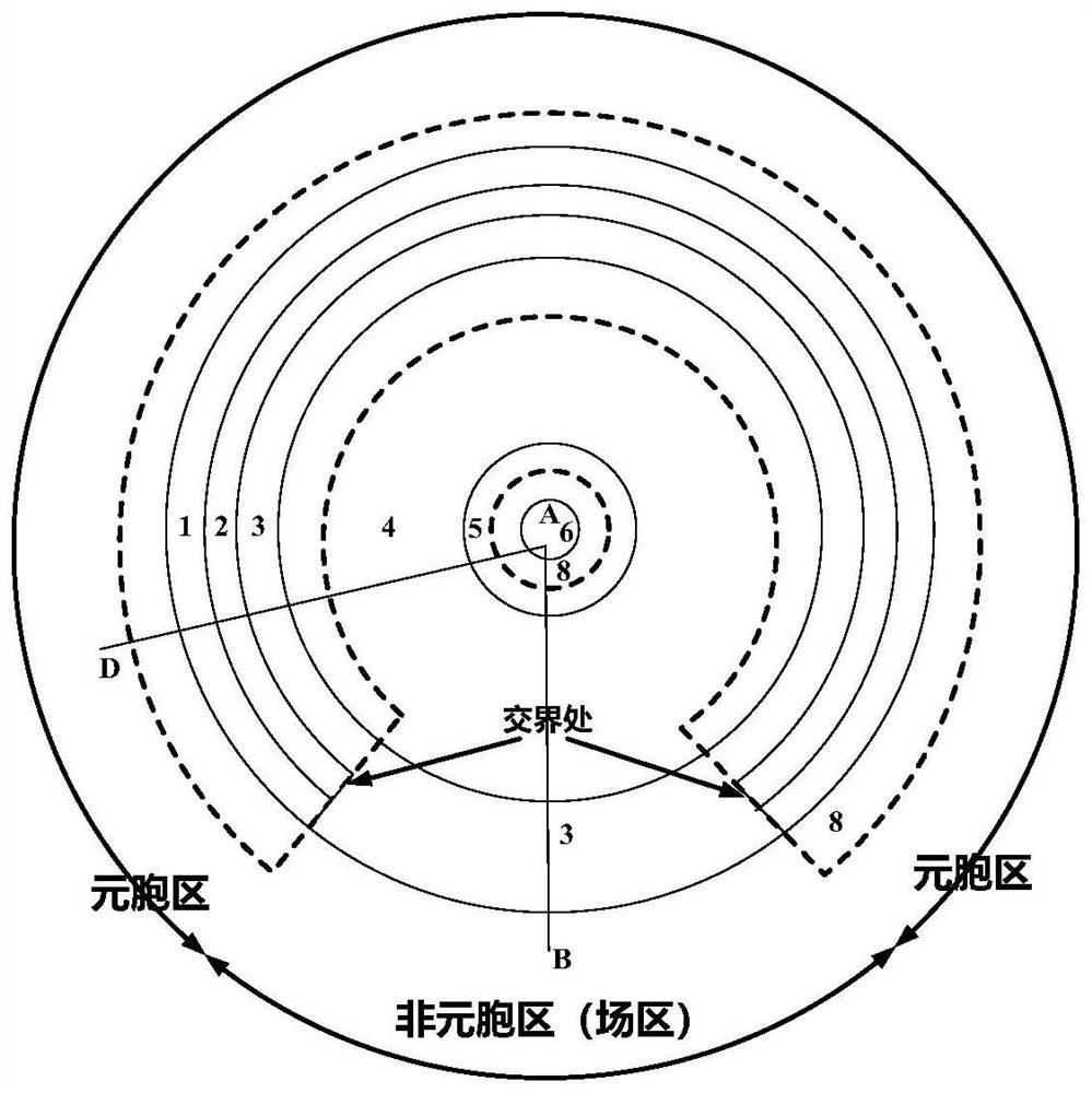
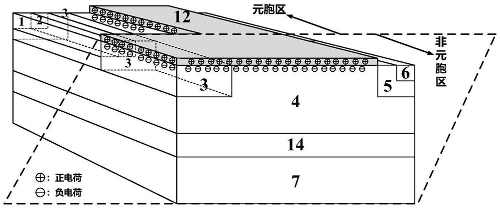
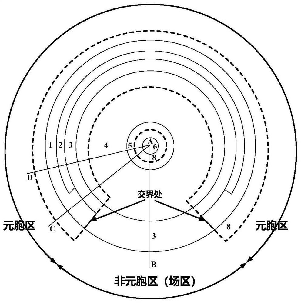
[0025] This embodiment provides a high-voltage LDMOS device structure with low radiation leakage, including three different cross-sectional structures of AB, AC and AD, wherein AB passes through the drain region 6 of the second conductivity type sequentially from the inside of the device along the radius to the outside, the active Region 8, the second conductivity type drift region 4 and the first conductivity type well region 3 direction; AC is from the inside of the device along the radius outwards through the second conductivity type drain region 6, the active region 8, and the second conductivity type drift region 4. The direction of the active region 8, the well region 3 of the first conductivity type and the body region 1 of the first conductivity type; direction of the conductivity type drift region 4 , the active region 8 , the first conductivity type well region 3 , the second conductivity type source region 2 and the first conductivity type body region 1 .

[0026] S...


PUM


Abstract

The invention provides a high-voltage LDMOS (Laterally Diffused Metal Oxide Semiconductor) device structure with low radiation electric leakage. The device comprises three different section structures of AB, AC and AD. Compared with a traditional high-voltage LDMOS device structure, an AC section structure is additionally arranged between an AB section and an AD section. A second conduction type source region is deleted from the junction of a cellular region and a non-cellular region (field region) to one side of the cellular region, namely an AC section, and a first conduction type body region extends rightwards to be tangent to the second conduction type source region in an AD section, so a radiation leakage path is cut off, the device leakage phenomenon caused by total dose radiation is avoided, off-state loss of the device is reduced, and total dose radiation resistance of the device is improved.

Description

technical field [0001] The invention belongs to the field of semiconductor power devices, in particular to a high-voltage LDMOS device structure with low radiation leakage. Background technique [0002] As power semiconductor devices are more and more widely used in aerospace electronic systems, for power management systems and gate drive circuits, anti-radiation hardening technology has become the research focus of various companies and universities. As the core part of the analog circuit, the high-voltage LDMOS device is characterized by occupying a large area and having a larger field oxide layer. Therefore, in the radiation environment such as γ-rays, LDMOS devices are prone to withstand voltage degradation, threshold drift and leakage current increase, which will increase the static power consumption of the circuit. In severe cases, the device will fail and the entire circuit cannot work normally. Radiation Leakage High Voltage LDMOS Devices. Contents of the inventio...

Claims


Application Information

Patent Timeline
Patent Type & Authority Applications(China)
IPC IPC(8): H01L29/78H01L23/552H01L29/10
CPCH01L29/7824H01L23/552H01L29/1095
Inventor 周锌耿立明王钊方雪淋师锐鑫乔明张波
Owner UNIV OF ELECTRONICS SCI & TECH OF CHINA
Why Eureka
Try Eureka