Segmentation and verification method, device, electronic device, storage medium

A technology to be divided and divided and processed, applied in the fields of electrical digital data processing, computer-aided design, instruments, etc., can solve the problems of division, time-consuming verification, increasing algorithm complexity, and low efficiency of chip design division and verification.

Active Publication Date: 2021-09-28
S2C
View PDF13 Cites 0 Cited by
  • Summary
  • Abstract
  • Description
  • Claims
  • Application Information

AI Technical Summary

Problems solved by technology

[0004] In the existing segmentation scheme, the chip design is usually segmented by using the segmentation algorithm. Although some segmentation requirements of users can be partially considered in the segmentation algorithm, the more and more personalized and flexible segmentation requirements of users not only increase The complexity of the algorithm, and the time-consuming process of segmentation and verification lead to low efficiency of segmentation and verification of the entire chip design, affecting the launch of integrated circuit products

Method used


Image

  • Segmentation and verification method, device, electronic device, storage medium
  • Segmentation and verification method, device, electronic device, storage medium
  • Segmentation and verification method, device, electronic device, storage medium

Examples


example 1

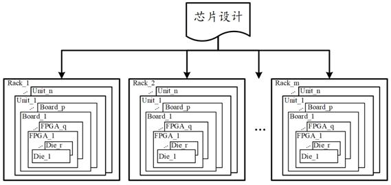
[0099] Example 1: Rack hierarchical segmentation.

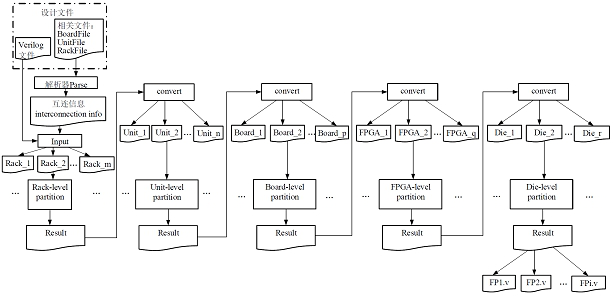
[0100] The basic unit of the Rack level is each Rack, which can be read into the file RackFile describing the Rack unit resources, port information, and interconnection information; then, the corresponding hypergraph data is designed, and the hypergraph data includes the resources required by each circuit node and the network. Connection relationship, node constraints and other information; Next, allocate the nodes with larger resource requirements among the nodes to different Racks as fixed nodes (fix nodes) in the Rack, and then consider the interconnection constraints between Racks, Carry out Rack level segmentation according to the minimum cut optimization objective, and obtain the segmentation results.

[0101] When interconnection constraints need to be considered during segmentation, it is necessary to consider the bit width characteristics of the interconnection interface between Racks, for example, a bidirectional tr...

example 2

[0108] Example 2: Unit level division.

[0109] The basic unit of the Unit level is each Unit, which can be read into the file UnitFile describing Unit unit resources, port information, and interconnection information, and the fixed node allocation information in each Unit obtained by Rack level segmentation; then, considering the interconnection constraints between Units, According to the minimum cut optimization objective, the Unit level segmentation is carried out to obtain the segmentation results. Similarly, when considering interconnection constraints, it is necessary to consider the bit width characteristics of the interconnection interface between Units.

[0110] After the division is completed, cross-Unit nets can be determined according to the obtained division results, so that the drive nodes in these nets can be fixed in specific Board units at the level below the Unit, that is, the Board level. The specific allocation method can be as follows: sort the cross-Unit...

example 3

[0116] Example 3: Board level division.

[0117] The basic unit of the Board level is each Board, which can first be read into the file BoardFile describing the Board unit resources, port information, and interconnection information, and the fixed node allocation information in each Board obtained by the division of the Unit level; then, considering the interconnection constraints between the Boards, According to the minimum cut optimization objective, the Board level segmentation is carried out to obtain the segmentation results. Similarly, when considering interconnection constraints, it is necessary to consider the bit width characteristics of the interconnection interface between boards.

[0118] After the segmentation is completed, cross-Board nets can be determined according to the obtained segmentation results, so as to fix the driving nodes in these nets in specific FPGA units at the next level of the Board, that is, the FPGA level. The specific allocation method can ...


PUM


Abstract

The embodiment of this specification provides a segmentation and verification method, device, electronic equipment, and storage medium, which are applied in the field of electronic design automation technology, wherein the segmentation method includes: dividing multiple segmentation levels according to the design level according to the design file corresponding to the design to be divided , and perform segmentation processing in each of the segmentation levels, and output the segmentation results. Through multi-level segmentation processing based on the design level, users can design custom groups to meet the user's personalized segmentation verification needs and improve the efficiency of segmentation verification.

Description

technical field [0001] The invention relates to the technical field of electronic design automation, in particular to a segmentation and verification method, device, electronic equipment, and storage medium. Background technique [0002] With the continuous improvement of chip integration and circuit complexity, a large chip design can often include hundreds of millions, billions or even tens of billions of gates, and a large number of IP cores, CPU cores, firmware code, microcontroller microcode, embedded software, etc. [0003] In the existing verification scheme, multiple verification chips, such as dozens or even hundreds of FPGAs (Field Programmable Gate Array, Field Programmable Gate Array), are used to form a multi-FPGA prototype verification system to verify a large-scale chip design. Split validation. [0004] In the existing segmentation scheme, the chip design is usually segmented by using the segmentation algorithm. Although some segmentation requirements of us...

Claims


Application Information

Patent Timeline
Patent Type & Authority Patents(China)
IPC IPC(8): G06F30/331G06F30/327
CPCG06F30/327G06F30/331
Inventor 李伟邵中尉万鹭张吉锋
Owner S2C
Why Eureka
Try Eureka