First-order electro-optical effect silicon modulator and preparation process thereof

A technology of electro-optical effect and preparation process, applied in the directions of light guide, optics, instruments, etc., can solve the problems of weak plasma dispersion effect, large device size, low modulation efficiency, etc., and achieve the effect of improving bandwidth, reducing insertion loss and improving modulation efficiency.

Pending Publication Date: 2021-08-20
SANMING UNIV
View PDF0 Cites 0 Cited by
  • Summary
  • Abstract
  • Description
  • Claims
  • Application Information

AI Technical Summary

Problems solved by technology

However, the plasmonic dispersion effect is still very weak, resulting in low modulation efficiency and large device size of the currently used silicon-based electro-optic modulators

Method used


Image

  • First-order electro-optical effect silicon modulator and preparation process thereof
  • First-order electro-optical effect silicon modulator and preparation process thereof
  • First-order electro-optical effect silicon modulator and preparation process thereof

Examples


Embodiment

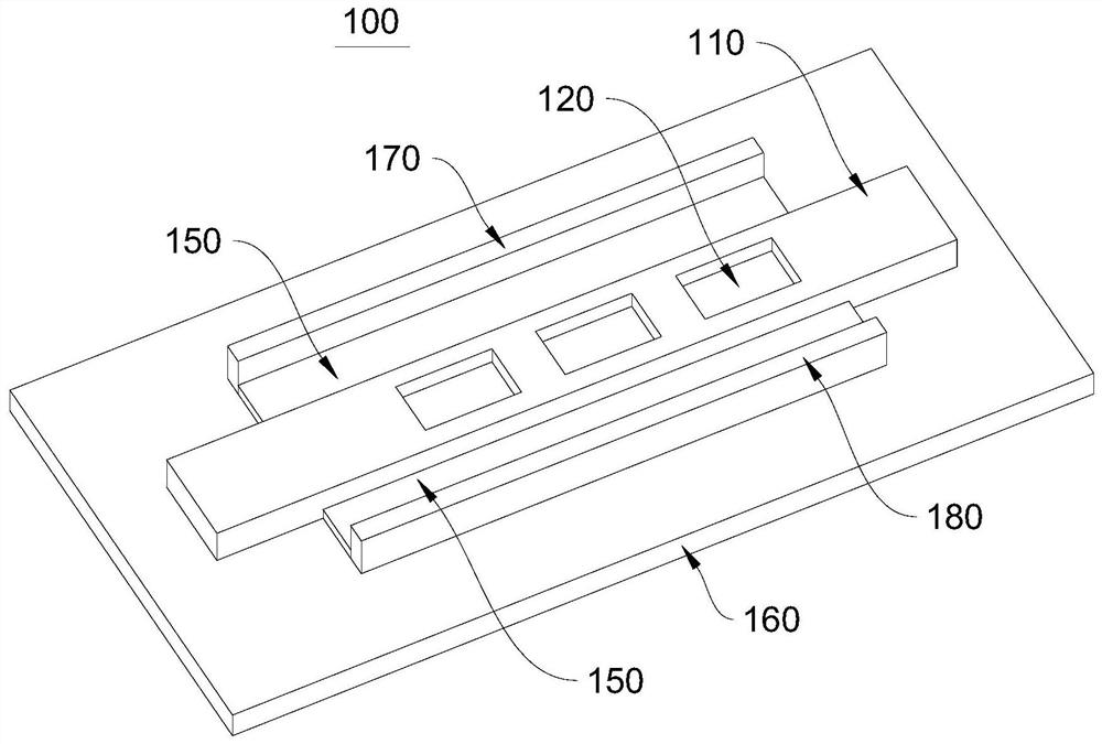
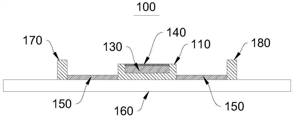
[0045] Please refer to figure 1 , figure 2 and image 3 This embodiment provides a preparation process of a first-order electro-optic effect silicon modulator 100, including:

[0046] The silicon waveguide region 110 is etched to form an amorphous silicon growth window 120, and the amorphous silicon growth window 120 is formed by etching of the upper surface of the silicon waveguide region 110.

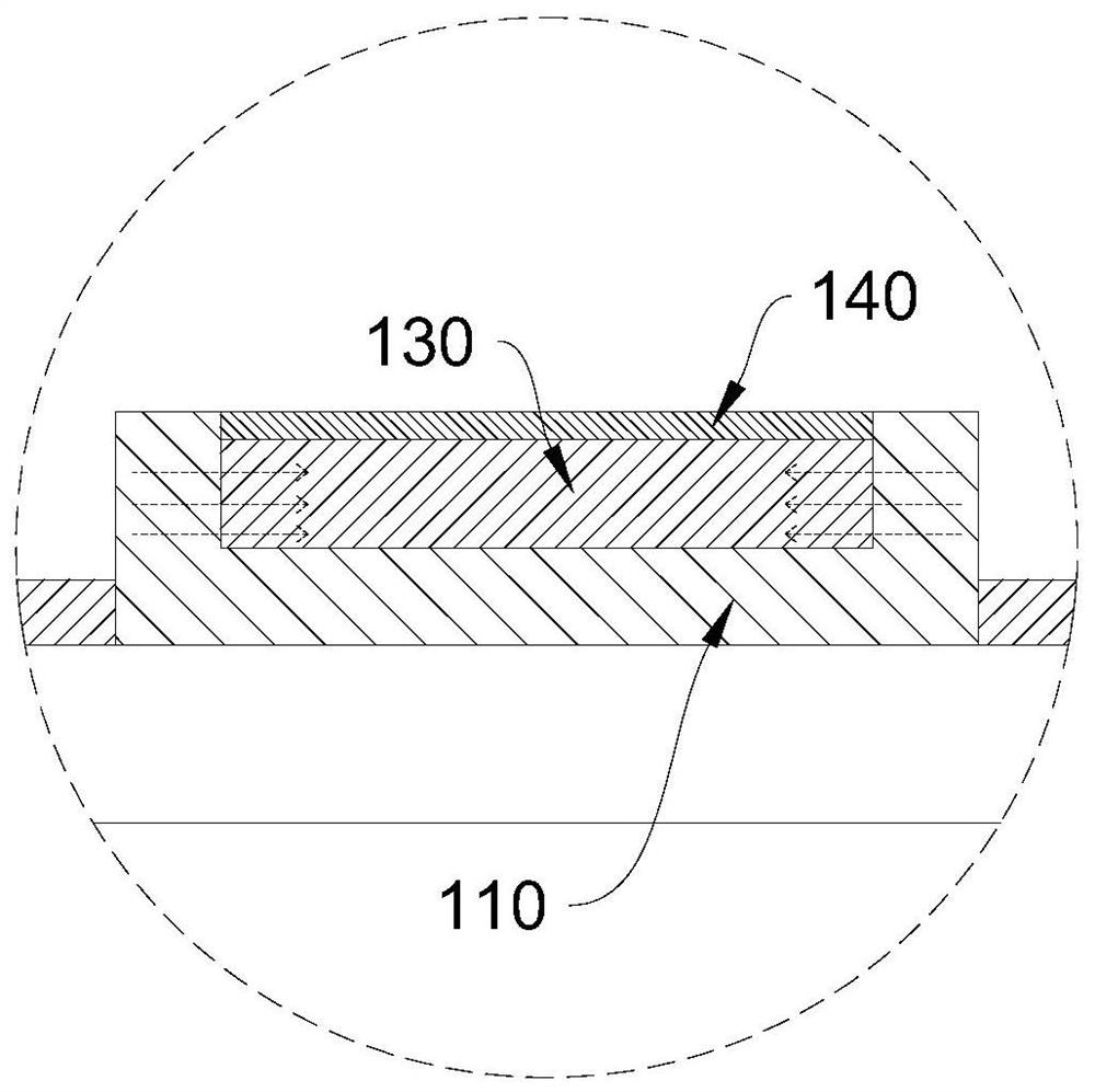
[0047] The amorphous silicon 130 is deposited in the amorphous silicon growth window 120, and the silicon dioxide layer 140 is covered with the surface of the deposited amorphous silicon 130.

[0048] The light irradiation amorphous silicon growth window 120 with a wavelength of 488 nm converts at least a portion of the amorphous silicon 130 in the amorphous silicon growth window 120 into single crystal silicon.

[0049] In the preparation process of first-order electro-optic effect silicon modulator 100, since the light energy of irradiation light having a wavelength of 488 nm is transpar...


PUM

PropertyMeasurementUnit
Wavelengthaaaaaaaaaa
Thicknessaaaaaaaaaa
Thicknessaaaaaaaaaa

Abstract

The invention discloses a first-order electro-optical effect silicon modulator and a preparation process thereof, and belongs to the field of electro-optical effect silicon modulators. The preparation process comprises the following steps that: a silicon waveguide region is etched to form an amorphous silicon growth window, wherein the amorphous silicon growth window is formed by etching the upper surface of the silicon waveguide region; amorphous silicon is deposited in the amorphous silicon growth window, and the surface of the deposited amorphous silicon is covered with a silicon dioxide layer; and the amorphous silicon growth window isirradiated with light with the wavelength of 488 nm to convert at least one part of the amorphous silicon in the amorphous silicon growth window into monocrystalline silicon. According to the prepared first-order electro-optical effect silicon modulator, the function limitation of a center inversion symmetric structure on the silicon-based electro-optical modulator is broken through by introducing asymmetric stress into the silicon structure, the modulation efficiency of the silicon-based modulator is greatly improved, the size of the device is effectively reduced, the bandwidth is improved, and the insertion loss is reduced.

Description

Technical field [0001] The present invention relates to the field of electro-optical effect silicon modulators, and in particular, a first-order electro-optic effect silicon modulator and a preparation process thereof. Background technique [0002] Silicon (Si) materials As the traditional material in the field of microelectronics, there is an unparalleled advantage of other materials in processing technology and manufacturing cost. Silicon-based light electronic devices have the advantages of easy integration, low process cost, etc., in recent years, the extensive attention of researchers. [0003] Although silicon-based optical electronic technology facing optical communication and optical interconnection has been well developed, but the silicon-based light electronics technology still has certain shortcomings in some respects due to the restrictions of the silicon material itself. [0004] As an important representative element in the silicon-based photoelectric integrated tec...

Claims


Application Information

Patent Timeline
IPC IPC(8): G02F1/025G02B6/12G02B6/13G02B6/136
CPCG02B6/12G02B6/13G02B6/136G02B2006/12061G02B2006/12142G02B2006/12171G02B2006/12176G02F1/025
Inventor 崔积适
Owner SANMING UNIV
Why Eureka
Try Eureka