Solar cell and passivation contact structure thereof, cell assembly and photovoltaic system

A technology of solar cells and contact structures, applied in the field of solar cells, can solve the problems of decreased conversion efficiency, poor isolation effect of conductive layers, increased compounding, etc.

Active Publication Date: 2021-08-20
ZHEJIANG AIKO SOLAR ENERGY TECH CO LTD
View PDF5 Cites 7 Cited by
  • Summary
  • Abstract
  • Description
  • Claims
  • Application Information

AI Technical Summary

Problems solved by technology

[0005] The purpose of the embodiments of the present invention is to provide a passivation contact structure for solar cells, which aims to solve the problems of poor isolation effect of the existing conductive layer and easy direct contact with the silicon substrate, resulting in increased recombination and decreased conversion efficiency.

Method used


Image

  • Solar cell and passivation contact structure thereof, cell assembly and photovoltaic system
  • Solar cell and passivation contact structure thereof, cell assembly and photovoltaic system
  • Solar cell and passivation contact structure thereof, cell assembly and photovoltaic system

Examples


Embodiment 1

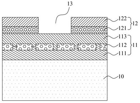
[0077] The embodiment of the present invention provides a passivation contact structure of a solar cell. For the convenience of description, only the parts related to the embodiment of the present invention are shown. Refer to figure 1 As shown, the passivation contact structure of the solar cell provided by the embodiment of the present invention includes:

[0078] a first passivation contact region 11 disposed on the silicon substrate 10, and a second passivation contact region 12 disposed on the first passivation contact region 11;

[0079] The second passivation contact region 12 has an opening 13, so that the conductive layer is connected to the first passivation contact region 11 through the opening 13;

[0080] The first passivation contact region 11 includes a first doped layer 111, a first passivation layer 112, and a second doped layer 113, and the second passivation contact region 12 includes a second passivation layer 121, and a third doped layer 113. Layer 122. ...

Embodiment 2

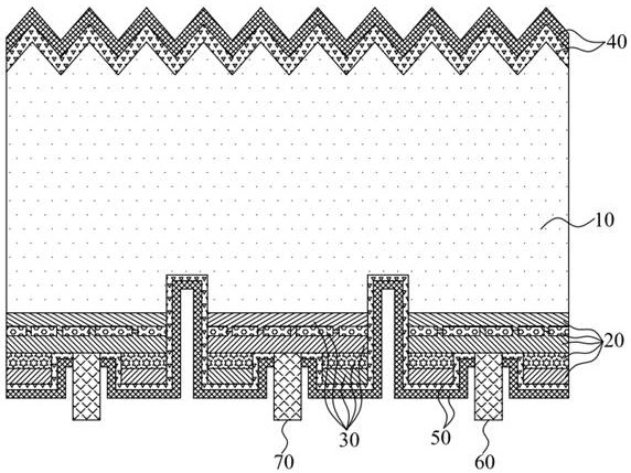
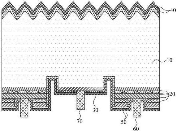
[0096] The second embodiment of the present invention provides a solar cell. For the convenience of description, only the parts related to the embodiment of the present invention are shown. Refer to Figure 2-Figure 11 As shown, the solar cell provided by the embodiment of the present invention includes:

[0097] silicon substrate 10;

[0098] The first doped region 20 and the second doped region 30 arranged at intervals on the back of the silicon substrate 10, the polarity of the first doped region 20 and the second doped region 30 are opposite;

[0099] a first dielectric layer 40 disposed on the front side of the silicon substrate 10;

[0100] a second dielectric layer 50 disposed between the first doped region 20 and the second doped region 30; and

[0101] a first conductive layer 60 disposed on the first doped region 20 and a second conductive layer 70 disposed on the second doped region 30;

[0102] Wherein, the first doped region 20 and / or the second doped region 30...

Embodiment 3

[0146] The third embodiment of the present invention provides a solar cell. For the convenience of description, only the parts related to the embodiment of the present invention are shown. Refer to Figure 12 As shown, the solar cell provided by the embodiment of the present invention includes:

[0147] silicon substrate 10;

[0148] The passivation contact structure 1 as described in the previous embodiment is arranged on the back side of the silicon substrate 10;

[0149] a third dielectric layer 80 disposed on the passivation contact structure 1;

[0150] a sixth doped layer 90 and a fourth dielectric layer 100 sequentially disposed on the front surface of the silicon substrate 10; and

[0151] a third conductive layer 110 electrically connected to the passivation contact structure 1 and a fourth conductive layer 120 electrically connected to the sixth doped layer 90;

[0152] Wherein the polarity of the passivation contact structure 1 is opposite to that of the sixth do...


PUM

PropertyMeasurementUnit
thicknessaaaaaaaaaa
thicknessaaaaaaaaaa
thicknessaaaaaaaaaa

Abstract

The invention is suitable for the technical field of solar cells, and provides a solar cell and a passivation contact structure thereof, a cell assembly and a photovoltaic system, the passivation contact structure comprises a first passivation contact area arranged on a silicon substrate and a second passivation contact area arranged on the first passivation contact area; the second passivation contact area is provided with an opening, so that the conductive layer is connected with the first passivation contact area; the first passivation contact area comprises a first doping layer, a first passivation layer and a second doping layer, the second passivation contact area comprises a second passivation layer and a third doping layer, and the first passivation layer is of a porous structure with the first doping layer and / or the second doping layer in a hole region. According to the passivation contact structure provided by the invention, the problems that an existing conducting layer is poor in isolation effect, and recombination is increased and conversion efficiency is reduced due to the fact that the existing conducting layer is easily in direct contact with a silicon substrate are solved.

Description

technical field [0001] The invention belongs to the technical field of solar cells, and in particular relates to a solar cell and its passivation contact structure, a cell component and a photovoltaic system. Background technique [0002] Solar cell power generation is a sustainable source of clean energy. It uses the photovoltaic effect of semiconductor p-n junctions to convert sunlight into electrical energy, and the conversion efficiency is an important indicator of solar cell performance. IBC (Interdigitated back contact) battery, that is, the interdigitated back contact battery, its positive / negative electrodes are designed on the back of the battery, so that the front surface completely avoids the shielding of the metal grid line, and eliminates the occlusion caused by the metal grid line. Optical loss, and the electrode width can be designed wider than the existing ones, which reduces the series resistance loss, thereby greatly improving the conversion efficiency. In...

Claims


Application Information

Patent Timeline
Patent Type & Authority Applications(China)
IPC IPC(8): H01L31/0224H01L31/0216H01L31/068
CPCH01L31/022441H01L31/022458H01L31/02167H01L31/02168H01L31/0682H01L31/0745H01L31/0747H01L31/0224H01L31/0216H01L31/074H01L31/0288H01L31/02366H01L31/022425H01L31/042H01L31/02363
Inventor 陈刚许文理邱开富王永谦杨新强
Owner ZHEJIANG AIKO SOLAR ENERGY TECH CO LTD
Why Eureka
Try Eureka