Preparation method of micro-fluidic chip detection device based on SERS substrate

A microfluidic chip and detection device technology, which is applied to measurement devices, chemical instruments and methods, laboratory containers, etc., can solve the problems of low practicability and effectiveness of Raman substrate detection, and achieve good detection functionality. , widely used, the effect of simple detection process

Inactive Publication Date: 2021-08-24
HEFEI UNIV OF TECH
View PDF9 Cites 3 Cited by
  • Summary
  • Abstract
  • Description
  • Claims
  • Application Information

AI Technical Summary

Problems solved by technology

[0006] At present, there is no use of microfluidic chip systems to solve the cumbersome and complicated operation methods of Raman detection using substrates, resulting in low practicability and effectiveness of Raman substrate detection. Therefore, we propose a SERS substrate-based The preparation method of the microfluidic chip detection device to solve the above problems

Method used


Image

  • Preparation method of micro-fluidic chip detection device based on SERS substrate
  • Preparation method of micro-fluidic chip detection device based on SERS substrate
  • Preparation method of micro-fluidic chip detection device based on SERS substrate

Examples


Embodiment

[0037] refer to Figure 1-4 , a method for preparing a microfluidic chip detection device based on a SERS substrate, comprising the following steps:

[0038] S1: spread PS pellets by solvent evaporation method;

[0039] S2: Utilize the liquid surface lifting method to transfer the PS spherical membrane;

[0040] S3: oxygen plasma etching;

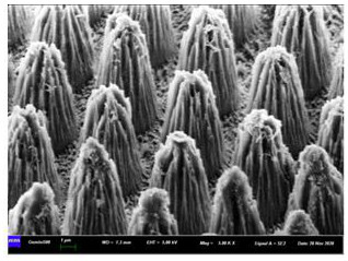
[0041] S4: Electron beam deposition of gold nanoparticles;

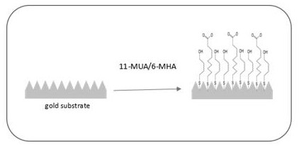
[0042] S5: Hydrophilic treatment of SERS substrate;

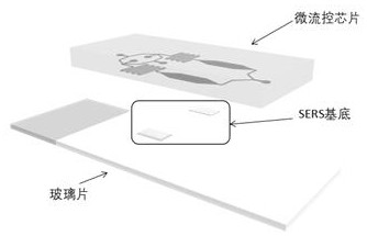
[0043] S6: Processing and manufacturing of microfluidic chips;

[0044] S7: Substrate embedding and chip sealing;

[0045] S8: Substrate characterization.

[0046] In this example, in S1, the glass slides to be used are cleaned, ultrasonically cleaned in acetone, ethanol and deionized water for 45 minutes, and then prepared with concentrated sulfuric acid and hydrogen peroxide at a ratio of 3:1 The mixed solution was used to clean the glass slices, and finally the glass slices were ultrasonically cleaned in a mixed solut...


PUM

PropertyMeasurementUnit
etching poweraaaaaaaaaa
thicknessaaaaaaaaaa
lengthaaaaaaaaaa

Abstract

The invention discloses a preparation method of a micro-fluidic chip detection device based on an SERS substrate, and relates to the field of surface Raman detection. The preparation method comprises the following steps: S1, paving PS pellets by utilizing a solvent evaporation method; S2, transferring the PS spherical membrane by using a liquid level pulling method; S3, performing oxygen plasma etching; S4, performing electron beam deposition of gold nanoparticles; S5, carrying out hydrophilic treatment on the SERS substrate; S6, processing and manufacturing the micro-fluidic chip; S7, embedding the substrate and sealing the chip; and S8, carrying out substrate characterization. The SERS substrate with the micro-nano heterostructure with the wrinkled micro-cones on the surface has a good Raman enhancement effect and good detection functionality, and the detection process is relatively simple; biochemical detection and analysis can be rapidly, conveniently and automatically carried out by coating the SERS substrate with the micro-fluidic chip, and the detection device can be more widely applied by combining the advantages of the two technologies.

Description

technical field [0001] The invention relates to the field of surface Raman detection, in particular to a preparation method of a microfluidic chip detection device based on a SERS substrate. Background technique [0002] The Raman scattering effect was discovered by C.V. Raman in an experiment in 1928. When light passes through a transparent medium in the experiment, part of the scattered light has a frequency different from that of the incident light. The theoretical explanation of Raman spectroscopy is that incident photons collide inelastically with molecules in the medium. When the frequency of photons absorbed by molecules is greater than the frequency of scattered photons, the scattering at this time is called Stokes scattering, also known as Raman scattering. However, the energy of Raman scattering is very small, and it is generally difficult to capture data. In 1977, the two research groups of Van Duyne and Creighton independently found that the Raman signal of eac...

Claims


Application Information

Patent Timeline
Patent Type & Authority Applications(China)
IPC IPC(8): G01N21/65G01N21/01B01L3/00
CPCG01N21/658G01N21/01B01L3/5027
Inventor 高荣科毛元朔杨玉杰
Owner HEFEI UNIV OF TECH
Why Eureka
Try Eureka