Micro ultraviolet light-emitting diode chip for ultraviolet communication
A light-emitting diode and communication technology, applied in semiconductor devices, electrical components, circuits, etc., can solve the problems of the optical power and external quantum efficiency of the device, improve the frequency response performance of the device, promote hole injection, and increase the hole concentration. Effect
- Summary
- Abstract
- Description
- Claims
- Application Information
AI Technical Summary
Problems solved by technology
Method used
Image

Examples
Embodiment 1
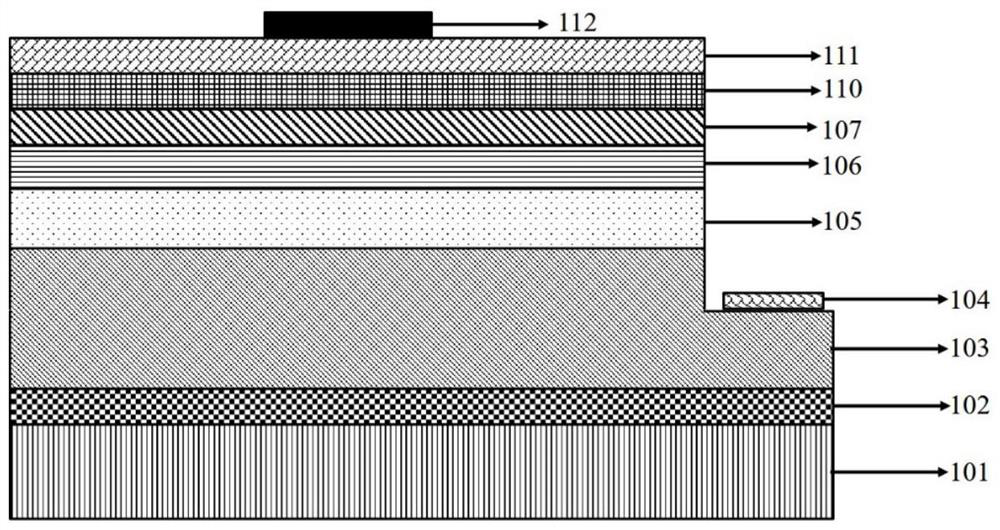
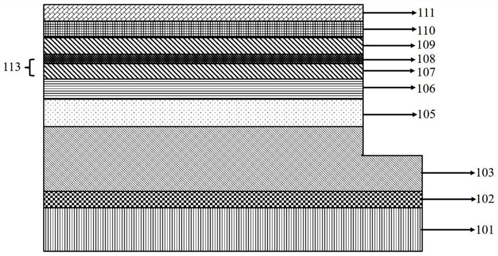
[0062]The micro ultraviolet light-emitting diode oriented to ultraviolet communication in this embodiment sequentially includes: a substrate 101, a buffer layer 102, and an n-type electron injection layer 103 along the epitaxial growth direction; the n-type electron injection layer 103 has a two-level stepped structure, The first step is the exposed part; the non-exposed part, that is, the second step of the n-type electron injection layer 103 is the multi-quantum well layer 105, the p-type electron blocking layer 106, and the first p-type hole along the epitaxial growth direction. Injection layer 107; the first p-type hole injection layer 107 is another two-level stepped structure, and the second-level step along the epitaxial growth direction is followed by a p-type hole acceleration layer 108, a second p-type hole Injection layer 109, p-type heavily doped hole injection layer 110, current spreading layer 111; p-type ohmic electrode 112 is arranged on the current spreading la...
Embodiment 2
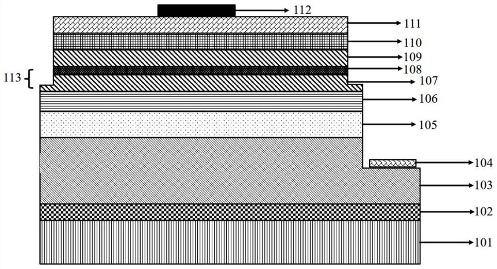
[0081] The micro ultraviolet light-emitting diode oriented to ultraviolet communication in this embodiment sequentially includes: a substrate 101, a buffer layer 102, and an n-type electron injection layer 103 along the epitaxial growth direction; the n-type electron injection layer 103 has a two-level stepped structure, The first step is the exposed part; the non-exposed part, that is, the second step of the n-type electron injection layer 103 is the multi-quantum well layer 105, the p-type electron blocking layer 106, and the first p-type hole along the epitaxial growth direction. Injection layer 107; the first p-type hole injection layer 107 is another two-level stepped structure, and the second-level step along the epitaxial growth direction is followed by a p-type hole acceleration layer 108, a second p-type hole Injection layer 109, p-type heavily doped hole injection layer 110, current spreading layer 111; p-type ohmic electrode 112 is arranged on the current spreading l...
PUM
| Property | Measurement | Unit |
|---|---|---|
| Thickness | aaaaa | aaaaa |
| Thickness | aaaaa | aaaaa |
| Thickness | aaaaa | aaaaa |
Abstract
Description
Claims
Application Information
 - R&D
- Intellectual Property
- Life Sciences
- Materials
- Tech Scout
- Unparalleled Data Quality
- Higher Quality Content
- 60% Fewer Hallucinations
Browse by: Latest US Patents, China's latest patents, Technical Efficacy Thesaurus, Application Domain, Technology Topic, Popular Technical Reports.
© 2025 PatSnap. All rights reserved.Legal|Privacy policy|Modern Slavery Act Transparency Statement|Sitemap|About US| Contact US: help@patsnap.com