Supercharge Your Innovation With Domain-Expert AI Agents!

Air gap manufacturing method, air gap and electronic equipment

A manufacturing method and technology of electronic equipment, applied in the direction of circuits, electrical components, electrical solid devices, etc., can solve the problems of reduced mechanical strength of the dielectric layer, unfavorable air gap shape and size, etc.

Inactive Publication Date: 2021-09-10
INST OF MICROELECTRONICS CHINESE ACAD OF SCI
View PDF3 Cites 0 Cited by
  • Summary
  • Abstract
  • Description
  • Claims
  • Application Information

AI Technical Summary

Problems solved by technology

In the current technology, a conductor layer is deposited on the dielectric layer, and then the dielectric layer is etched to form an air gap. However, the air gap prepared by this process is not conducive to controlling the shape and size of the air gap, and on the other hand, it is easy lead to a decrease in the mechanical strength of the dielectric layer

Method used


Image

  • Air gap manufacturing method, air gap and electronic equipment
  • Air gap manufacturing method, air gap and electronic equipment
  • Air gap manufacturing method, air gap and electronic equipment

Examples


preparation example Construction

[0062] In the preparation method of the air gap 10 provided by the present invention, after the groove 3 is formed by etching on the first dielectric layer 2, it is not necessary to remove other photoresist layers 5 that have not been removed immediately, and can be directly on the photoresist layer 5. Filling the conductive material in the trench 3 can simplify the process steps and reduce the process cost.

[0063] The height of the air gap is adjusted by adjusting the ratio of the thickness of the photoresist and the dielectric layer, so as to facilitate the control of the height of the air gap 10 .

[0064] Such as Figure 5 to Figure 8 As shown, in some examples, the step of filling the trench 3 with a conductive material and forming the bridging structure 4 includes: sequentially depositing a barrier layer 6 and a seed layer 7 in the trench 3 and on another part of the photoresist layer 5; Fill the conductive material on the seed layer 7; remove the barrier layer 6, the...

specific Embodiment 1

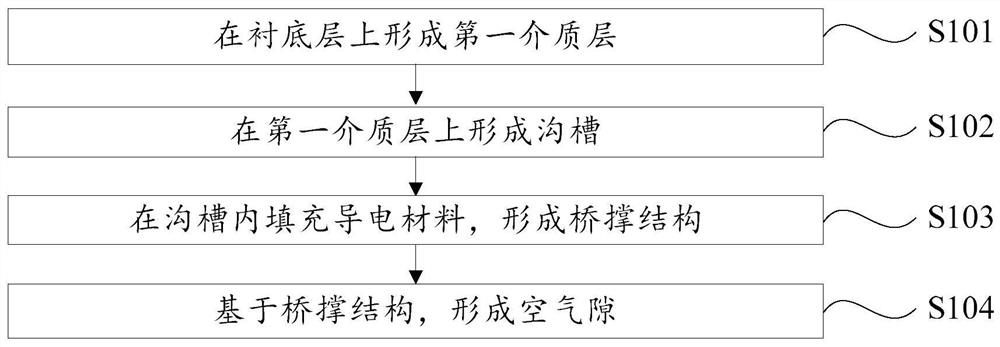
[0087] Such as Figure 2 to Figure 9 with Figure 17 As shown, this embodiment provides a method for manufacturing an air gap, including:

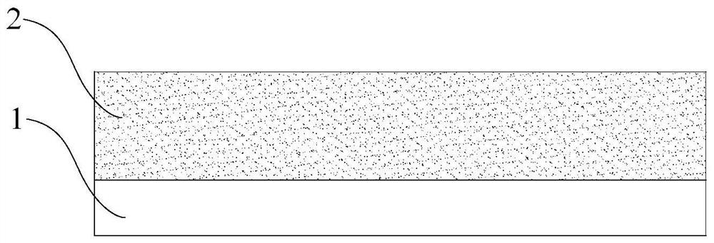
[0088] Step S201: forming a first dielectric layer on the substrate layer;

[0089] Step S201: forming a first dielectric layer on the substrate layer;

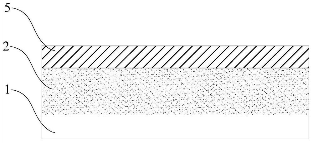
[0090] Step S202: setting a photoresist layer on the first dielectric layer;

[0091] Step S203: removing part of the photoresist layer through an exposure and development process, and removing part of the first dielectric layer through an etching process to form a trench;

[0092] Step S204: filling the trench and another part of the photoresist layer with conductive material;

[0093] Step S205: removing the conductive material on another part of the photoresist layer by etching or chemical mechanical polishing;

[0094] Step S206: Etching another part of the photoresist layer to form a bridge structure;

[0095] Step S207: Depositing a second dielectric layer on the bridging stru...

specific Embodiment 2

[0099] Such as Figure 10 to Figure 16 with Figure 18 As shown, this embodiment provides a method for manufacturing an air gap, including:

[0100] Step S301: forming a first dielectric layer on the substrate layer;

[0101] Step S302: setting a photoresist layer on the first dielectric layer;

[0102] Step S303: Etching part of the photoresist layer and part of the first dielectric layer by a photolithography process to form a trench;

[0103] Step S304: sequentially depositing a barrier layer and a seed layer in the trench and on another part of the photoresist layer;

[0104] Step S305: filling the seed layer with conductive material;

[0105] Step S306: removing the barrier layer, seed layer and conductive material on another part of the photoresist layer by etching or chemical mechanical polishing;

[0106] Step S307: etching another part of the photoresist layer to form a bridge structure;

[0107] Step S308: depositing a liner layer on the bridge structure and the ...


PUM


Abstract

The embodiment of the invention provides an air gap manufacturing method, an air gap and electronic equipment. The air gap manufacturing method comprises the steps: forming a first dielectric layer on a substrate layer; forming a groove on the first dielectric layer; filling the groove with a conductive material to form a bridge support structure; and forming an air gap based on the bridge support structure, wherein a part of the bridge support structure extends out of the groove. According to the air gap manufacturing method provided by the invention, a groove is etched in a first dielectric layer, and is filled with a conductor material to form a bridge support structure, so that the size of the air gap can be controlled by controlling the filling height of the conductor material, the shape of the air gap can be controlled by controlling the shape of the groove, and the air gap can be formed without performing secondary etching on the dielectric layer so as to improve the mechanical strength of the dielectric layer.

Description

technical field [0001] The invention relates to the technical field of semiconductors, in particular to an air gap manufacturing method, an air gap and an electronic device. Background technique [0002] With the development of semiconductor technology, the size of the internal interconnection of the chip is continuously reduced, resulting in the delay of interconnection resistance and capacitance becoming the main factor restricting the development of devices. Currently the most commonly used interconnection process in the industry is a copper interconnection process with a Ta / TaN barrier layer. As the size decreases, the grain boundary scattering and surface scattering of electrons in the interconnect line intensify, resulting in a sharp increase in the resistivity of copper. The thickness of the Ta / TaN barrier layer cannot be further reduced, resulting in a further reduction in the size of the copper in the interconnection lines and vias, and the resistivity of the barri...

Claims


Application Information

Patent Timeline
Patent Type & Authority Applications(China)
IPC IPC(8): H01L21/768H01L23/532
CPCH01L21/7682H01L21/76877H01L21/76802H01L23/53295
Inventor 孙祥烈许静罗军赵超
Owner INST OF MICROELECTRONICS CHINESE ACAD OF SCI
Features
  • R&D
  • Intellectual Property
  • Life Sciences
  • Materials
  • Tech Scout
  • Unparalleled Data Quality
  • Higher Quality Content
  • 60% Fewer Hallucinations
Learn More