Semiconductor structure and method of forming the same

A semiconductor and measurement method technology, applied in the direction of semiconductor devices, semiconductor/solid-state device manufacturing, semiconductor/solid-state device components, etc., can solve the problem of affecting test signal strength and integrity, lower wafer pass rate, and inaccurate wafer marking and other problems, to achieve the effect of improving overlay accuracy, improving flatness and completeness

Active Publication Date: 2022-07-26
YANGTZE MEMORY TECH CO LTD
View PDF4 Cites 0 Cited by
  • Summary
  • Abstract
  • Description
  • Claims
  • Application Information

AI Technical Summary

Problems solved by technology

The height difference between the 3D storage device and its surrounding dicing lines is more obvious. The higher the number of layers of the storage device near the dicing line, the higher the height of the photoresist layer on it, and the photoresist layer above the alignment mark in the dicing line Therefore, the profile of the photoresist layer above the alignment mark is uneven, which affects the strength and integrity of the test signal of the alignment mark, and the marking of the wafer is not accurate, resulting in a large Measurement errors lead to poor overlay accuracy (overlay, OVL), lower wafer pass rate; and, when the test signal is weak, the wafer may be misjudged as a non-qualified wafer, resulting in waste
[0004] In the prior art, the flatness of the photoresist is improved by slowing down the spin coating speed of the photoresist, but the effect is still unsatisfactory. After slowing down the spin coating speed, the wafer WPH (wafer per hour, output rate per hour) decreases ; and there is still residual (residual overlay performance indicator, ROPI) overlay error after correction

Method used


Image

  • Semiconductor structure and method of forming the same
  • Semiconductor structure and method of forming the same
  • Semiconductor structure and method of forming the same

Examples


Embodiment Construction

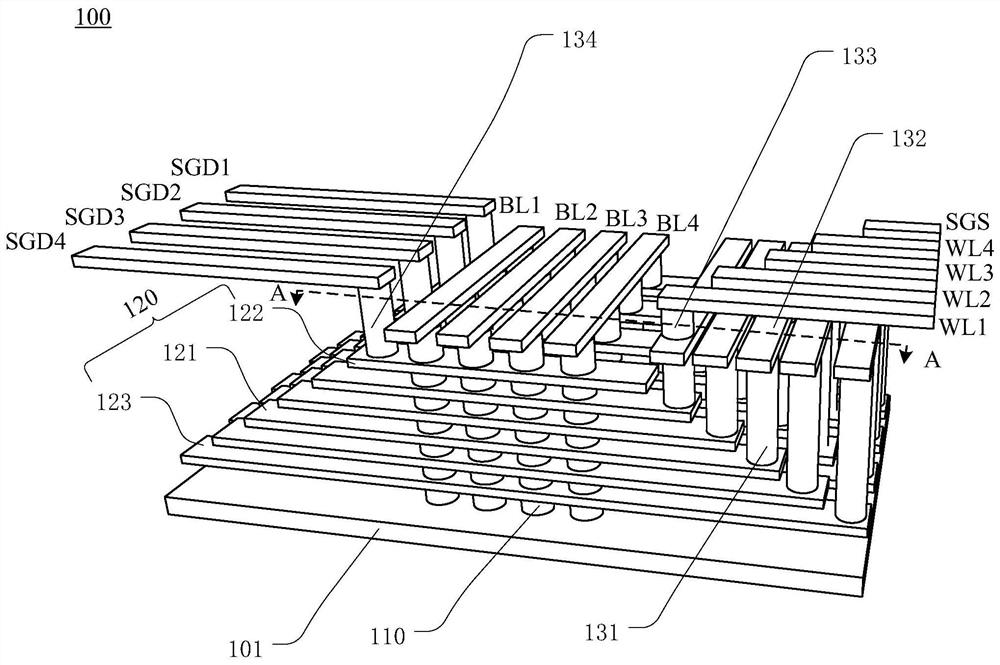
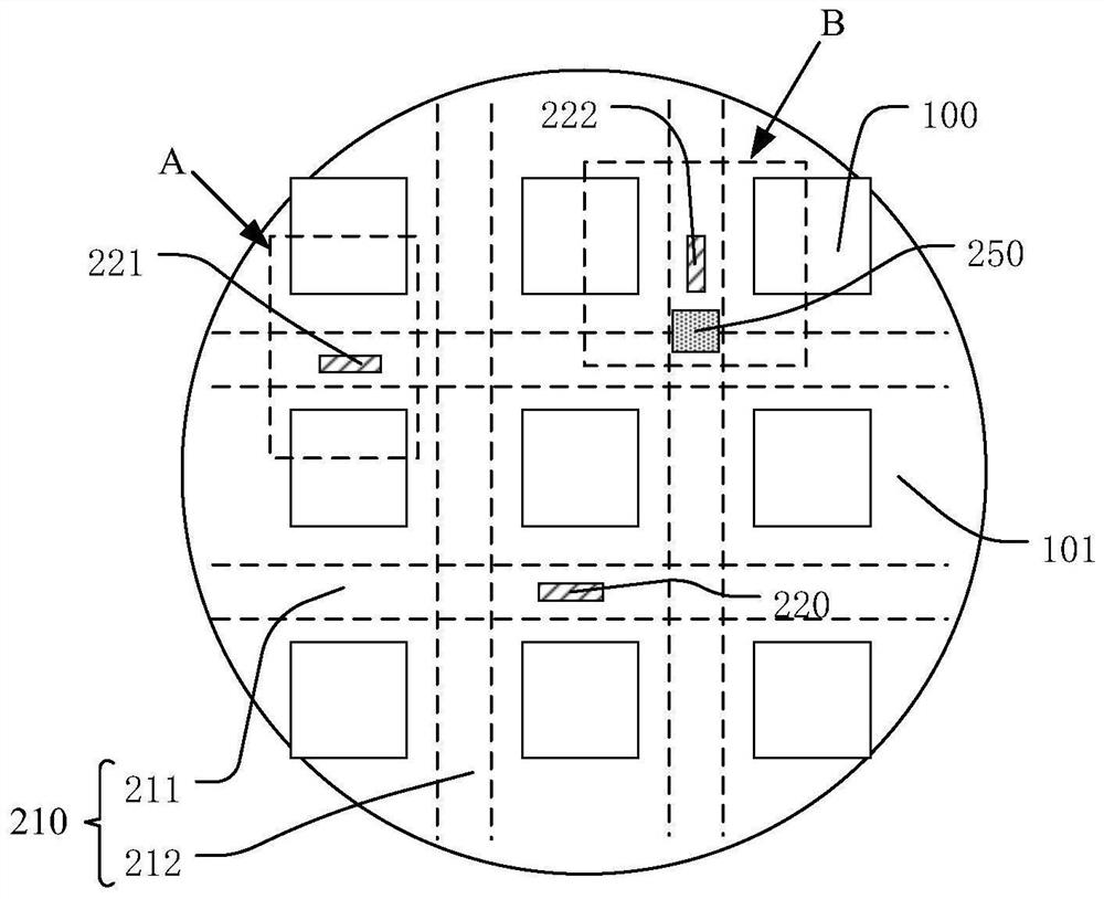
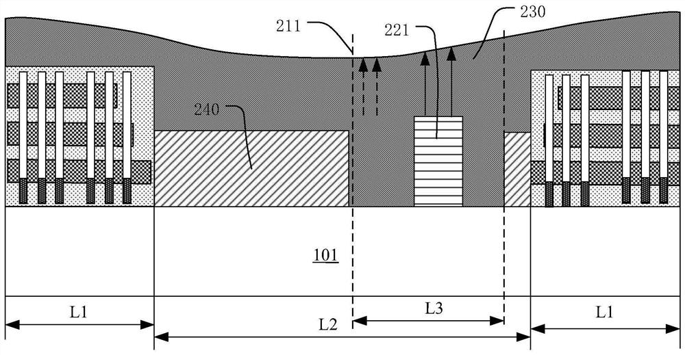
[0046] The present invention will be described in more detail below with reference to the accompanying drawings. In the various figures, like elements are designated by like reference numerals. For the sake of clarity, various parts in the figures have not been drawn to scale. Additionally, some well-known parts may not be shown. For the sake of brevity, a semiconductor structure obtained after several steps, including all layers or regions that have been formed, may be depicted in one figure.

[0047] It will be understood that, in describing the structure of a device, when a layer or region is referred to as being "on" or "over" another layer or region, it can be directly on the other layer or region, or Other layers or regions are also included between it and another layer, another region. And, if the device is turned over, the layer, one region, will be "under" or "under" another layer, another region.

[0048] The invention may be embodied in various forms, some examp...


PUM


Abstract

The present application discloses a semiconductor structure and a method for forming the same. The semiconductor structure includes: a substrate; a plurality of storage areas, wherein the plurality of storage areas are arranged in an array on the substrate to form a storage device; and a plurality of scribe lines , each of the dicing lanes is located between two adjacent storage areas; alignment marks, located in the dicing lanes, are formed on the substrate, close to the center of the two storage areas; photolithography Glue, over the storage area and the scribe line, covers the alignment marks. The alignment mark is set at a position close to the middle of the two adjacent storage areas, and the photoresist above the position is relatively flat, so that the intensity of the measurement signal of the alignment mark measured through the photoresist is higher, and the The engraving accuracy is improved, the measurement error is small, the wafer pass rate is high, and the cost is reduced.

Description

technical field [0001] The present invention relates to the technical field of semiconductor manufacturing, and more particularly, to a semiconductor structure and a method for forming the same. Background technique [0002] As the feature sizes of semiconductor manufacturing processes are getting smaller and smaller, the storage density of memory devices is getting higher and higher. In order to further increase the storage density, three-dimensionally structured storage devices (ie, 3D storage devices) have been developed. 3D memory devices include multiple memory cells stacked in a vertical direction, which can exponentially increase the level of integration on a wafer per unit area, and can reduce costs. [0003] At present, 3D memory devices are stacked with more and more memory cells, corresponding to more and more semiconductor layers, and the height of the semiconductor structures formed on the wafer is getting higher and higher, and the step height of the effective...

Claims


Application Information

Patent Timeline
Patent Type & Authority Patents(China)
IPC IPC(8): G03F9/00G03F7/20H01L23/544H01L21/304H01L21/027H01L27/11519H01L27/11556H01L27/11565H01L27/11582
CPCG03F9/7073G03F9/7076G03F7/70633H01L23/544H01L21/3043H01L21/0271H01L2223/54426H10B41/10H10B41/27H10B43/10H10B43/27
Inventor 方超魏禹农陈航卫袁元
Owner YANGTZE MEMORY TECH CO LTD
Why Eureka
Try Eureka