Metal bump packaging structure and manufacturing method thereof
A technology of packaging structure and metal bumps, which is used in semiconductor/solid-state device manufacturing, semiconductor/solid-state device parts, semiconductor devices, etc. It can avoid problems such as poor welding effect, and achieve the effect of avoiding the falling of welding bumps, high structural stability and improving surface roughness.
- Summary
- Abstract
- Description
- Claims
- Application Information
AI Technical Summary
Problems solved by technology
Method used
Image
Examples
no. 1 example
[0051] see in conjunction figure 1 and figure 2 , this embodiment provides a metal bump packaging structure 100, which can improve the reliability of the packaging structure, and at the same time, the structural stability of the product is relatively high.
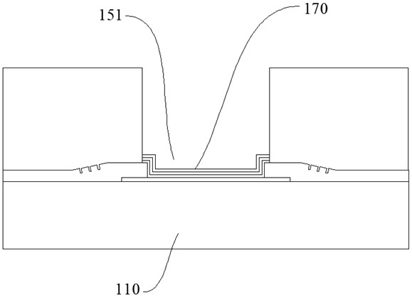
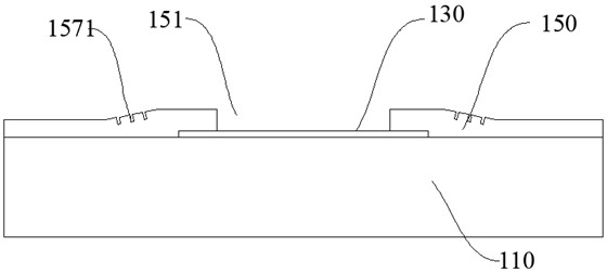
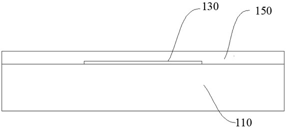
[0052] The metal bump packaging structure 100 provided in this embodiment includes a substrate chip 110, a conductive pad 130, a protective layer 150, a metal conductive layer 170, and a welding bump 190, and the conductive pad 130 is disposed on the surface of the substrate chip 110. The protective layer 150 is disposed on the surface of the substrate chip 110, and the protective layer 150 is provided with a pad opening 151, the pad opening 151 corresponds to the conductive pad 130, so that at least part of the surface of the conductive pad 130 is located in the pad opening 151 inside, so that the conductive pad 130 is exposed to the protective layer 150, the metal conductive layer 170 is arranged on the surface of the ...
no. 2 example
[0067] see Figure 4 , this embodiment provides a metal bump packaging structure 100, its basic structure and principle and the technical effect produced are the same as those of the first embodiment, for a brief description, for the part not mentioned in this embodiment, please refer to the first Corresponding content in the embodiment.
[0068] In this embodiment, the metal bump packaging structure 100 includes a substrate chip 110, a conductive pad 130, a protective layer 150, a metal conductive layer 170, and a welding bump 190, and the conductive pad 130 is disposed on the surface of the substrate chip 110, The protective layer 150 is disposed on the surface of the substrate chip 110, and the protective layer 150 is provided with a pad opening 151, the pad opening 151 corresponds to the conductive pad 130, so that at least part of the surface of the conductive pad 130 is located in the pad opening 151 inside, so that the conductive pad 130 is exposed to the protective la...
no. 3 example
[0071] see Figure 5 , this embodiment provides a metal bump packaging structure 100, its basic structure and principle and the technical effect produced are the same as those of the first embodiment, for a brief description, for the part not mentioned in this embodiment, please refer to the first Corresponding content in the embodiment.
[0072] In this embodiment, the metal bump packaging structure 100 includes a substrate chip 110, a conductive pad 130, a protective layer 150, a metal conductive layer 170, and a welding bump 190, and the conductive pad 130 is disposed on the surface of the substrate chip 110, The protective layer 150 is disposed on the surface of the substrate chip 110, and the protective layer 150 is provided with a pad opening 151, the pad opening 151 corresponds to the conductive pad 130, so that at least part of the surface of the conductive pad 130 is located in the pad opening 151 inside, so that the conductive pad 130 is exposed to the protective la...
PUM
| Property | Measurement | Unit |
|---|---|---|
| thickness | aaaaa | aaaaa |
| thickness | aaaaa | aaaaa |
Abstract
Description
Claims
Application Information


