Transparent antenna preparation method based on film photoetching process and transparent antenna
A transparent and antenna technology, applied in the direction of radiating element structure, conductive pattern formation, etc., can solve the problems of operator health hazards, difficulty in achieving concealment, waste liquid pollution, etc. the effect
- Summary
- Abstract
- Description
- Claims
- Application Information
AI Technical Summary
Problems solved by technology
Method used
Image
Examples
Embodiment 1
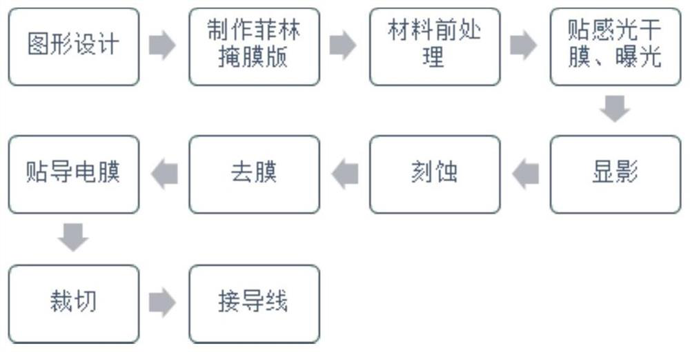
[0041] This embodiment provides a method for preparing a transparent antenna based on a film lithography process, and the basic steps are as follows:
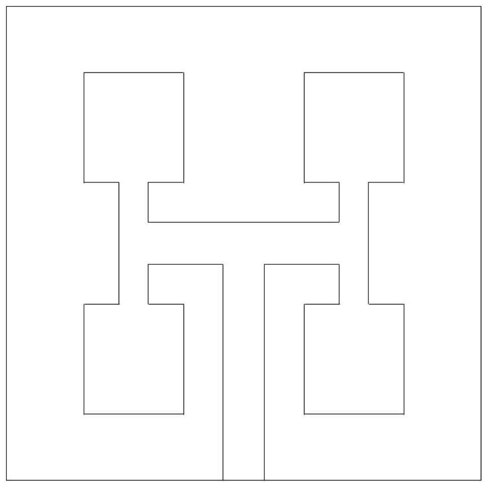
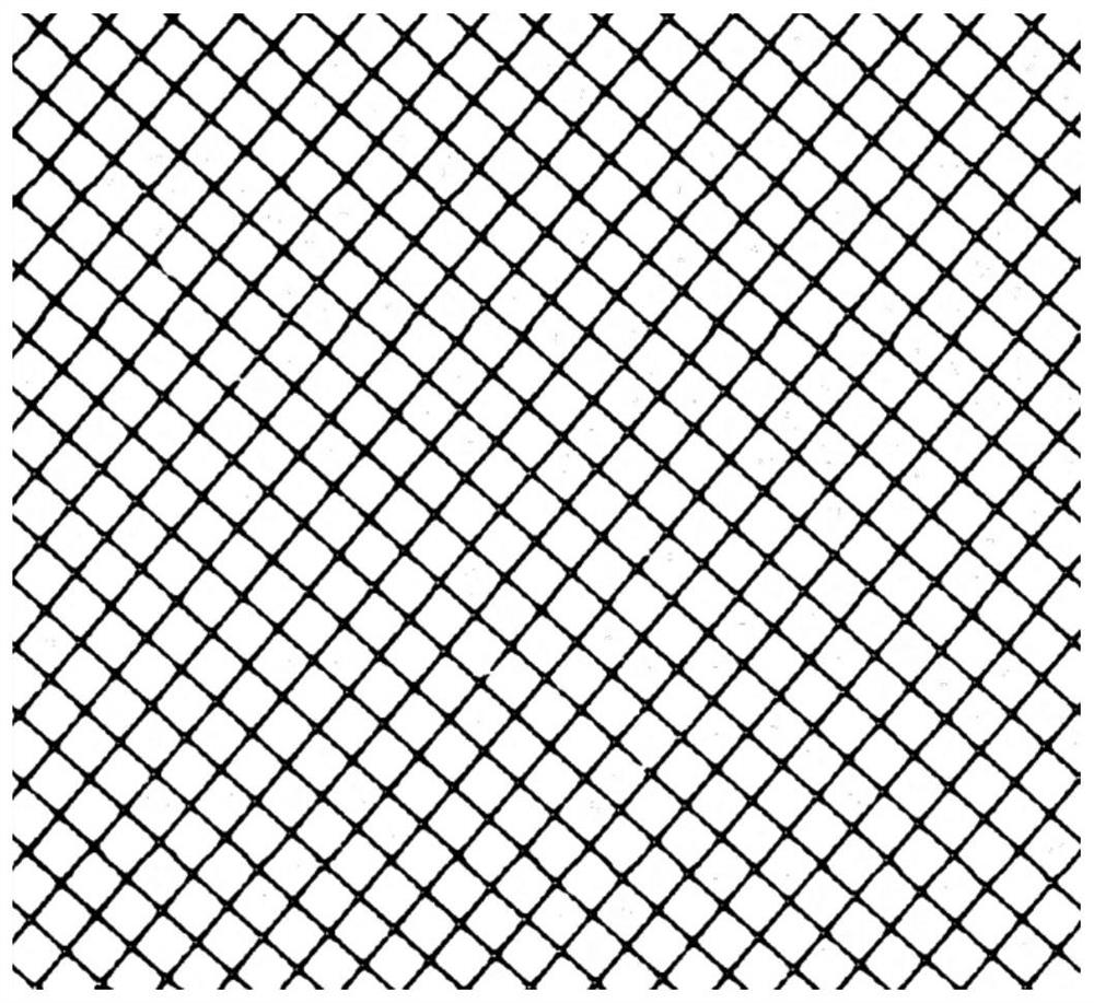
[0042] S1. Design of low visibility transparent antenna structure;
[0043] S2. Draw the low-visibility transparent antenna structure graph, and output the low-visibility transparent antenna structure graph on the film sheet to make a film mask;
[0044] S3. Cutting the transparent conductive film and the photosensitive dry film to a predetermined size and pre-processing;
[0045] S4. Paste the photosensitive dry film on the surface of the transparent conductive film, and expose the conductive film pasted with the photosensitive dry film;
[0046] S5. developing to expose the structural pattern of the transparent antenna;
[0047] S6. Etching out the shape of the transparent antenna by etching solution;
[0048] S7. removing the photosensitive dry film on the surface of the transparent conductive film and washing and drying ...
Embodiment 2
[0065] This embodiment provides a method for preparing a transparent antenna based on a film lithography process, and the basic steps are as follows:
[0066] S1. Design of low visibility transparent antenna structure;
[0067] S2. Output the low-visibility transparent antenna structure pattern onto the film sheet to make a film mask;
[0068] S3. Cutting the transparent conductive film and the photosensitive dry film to a predetermined size and pre-processing;
[0069] S4. Paste the photosensitive dry film on the surface of the transparent conductive film, and expose the conductive film pasted with the photosensitive dry film;
[0070] S5. developing to expose the structural pattern of the transparent antenna;
[0071] S6. Etching out the shape of the transparent antenna by etching solution;
[0072] S7. removing the photosensitive dry film on the surface of the transparent conductive film and washing and drying to obtain the required transparent conductive film;
[0073]...
PUM
| Property | Measurement | Unit |
|---|---|---|
| width | aaaaa | aaaaa |
| width | aaaaa | aaaaa |
| width | aaaaa | aaaaa |
Abstract
Description
Claims
Application Information
 - R&D Engineer
- R&D Manager
- IP Professional
- Industry Leading Data Capabilities
- Powerful AI technology
- Patent DNA Extraction
Browse by: Latest US Patents, China's latest patents, Technical Efficacy Thesaurus, Application Domain, Technology Topic, Popular Technical Reports.
© 2024 PatSnap. All rights reserved.Legal|Privacy policy|Modern Slavery Act Transparency Statement|Sitemap|About US| Contact US: help@patsnap.com


