Supercharge Your Innovation With Domain-Expert AI Agents!

Preparation method of led epitaxy, led epitaxy structure and led chip

An epitaxial structure and epitaxial technology, applied in the direction of semiconductor devices, electrical components, nanotechnology, etc., can solve the problems that it is difficult to obtain high-efficiency GaN-based Micro and Mini LEDs with high In composition, to reduce stress, increase overlapping areas, Effect of Polarization Improvement

Active Publication Date: 2022-05-03
CHONGQING KONKA PHOTOELECTRIC TECH RES INST CO LTD
View PDF2 Cites 0 Cited by
  • Summary
  • Abstract
  • Description
  • Claims
  • Application Information

AI Technical Summary

Problems solved by technology

[0005] In view of the above deficiencies in the prior art, the purpose of the present invention is to provide a method for preparing LED epitaxy and an LED epitaxy structure, aiming to solve the problem that it is difficult to obtain high-efficiency GaN-based Micro and Mini LEDs with high In composition.

Method used


Image

  • Preparation method of led epitaxy, led epitaxy structure and led chip
  • Preparation method of led epitaxy, led epitaxy structure and led chip
  • Preparation method of led epitaxy, led epitaxy structure and led chip

Examples


Embodiment Construction

[0031] The present invention provides a method for preparing LED epitaxy, an LED epitaxy structure and an LED chip. In order to make the purpose, technical solution and effect of the present invention clearer and clearer, the present invention will be further described in detail below. It should be understood that the specific embodiments described here are only used to explain the present invention, not to limit the present invention.

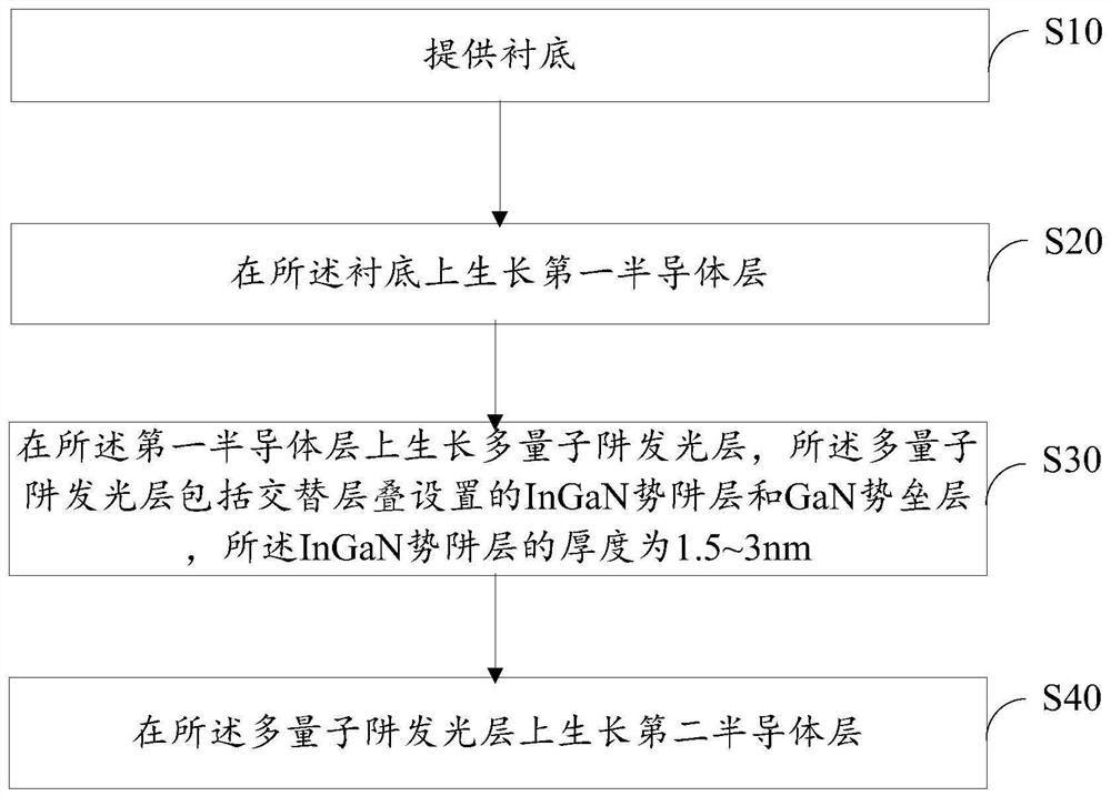
[0032] Embodiments of the present invention provide a method for preparing LED epitaxy, such as figure 1 As shown, the method includes:

[0033] S10, providing a substrate;

[0034] S20, growing a first semiconductor layer on the substrate;

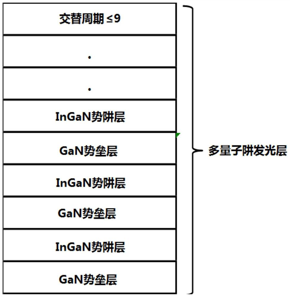
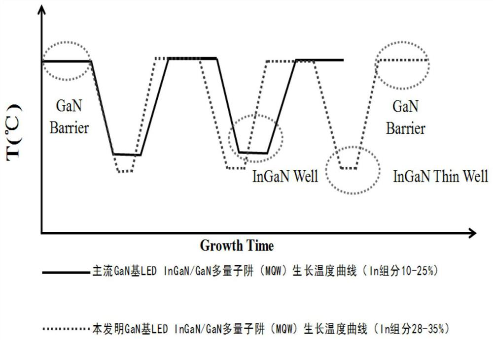
[0035] S30. Growing a multi-quantum well light-emitting layer on the first semiconductor layer, the multi-quantum well light-emitting layer comprising alternately stacked InGaN potential well layers and GaN barrier layers (see figure 2 shown), the thickness of the InGaN potential well layer is 1.5-3nm...


PUM

PropertyMeasurementUnit
thicknessaaaaaaaaaa
thicknessaaaaaaaaaa
temperatureaaaaaaaaaa

Abstract

The invention discloses an LED epitaxial preparation method, an LED epitaxial structure and an LED chip. The method includes: providing a substrate; growing a first semiconductor layer on the substrate; growing a multi-quantum well light-emitting layer on the first semiconductor layer, and the multi-quantum well light-emitting layer includes alternately stacked InGaN potential A well layer and a GaN barrier layer, the thickness of the InGaN potential well layer is 1.5-3nm; a second semiconductor layer is grown on the multi-quantum well light-emitting layer. In the present invention, by thinning the thickness of the InGaN potential well layer, the increase of In composition in the InGaN potential well layer can be realized at a lower growth temperature. The invention adopts the ultra-thin InGaN potential well layer, which can reduce the stress caused by the lattice mismatch between the InGaN potential well layer and the GaN barrier layer, improve the polarization, and effectively increase the overlapping area of ​​the electron and hole wave functions. Finally, a GaN-based LED with high internal quantum efficiency in the long wavelength band is obtained.

Description

technical field [0001] The present invention relates to the field of semiconductors, in particular to a method for preparing a light-emitting diode (Light-Emitting Diode, LED for short) epitaxy, an LED epitaxy structure and an LED chip. Background technique [0002] At present, the mainstream GaN (gallium nitride)-based Micro (micro) and Mini LED (mini LED) are based on the structure of multiple quantum wells (Multiple Quantum Well, abbreviated as MQW). The multiple quantum well light-emitting area is composed of InGaN ( InGaN) potential well layer (Well) and GaN barrier layer (Barrier) are grown alternately periodically, and the multi-quantum well light-emitting region is the core region where carriers undergo radiative recombination and luminescence. The InGaN potential well layer has a smaller width and a narrower band gap, and will form a quantum well energy band structure with the GaN barrier layer in the multi-quantum well light-emitting region. This structure can make...

Claims


Application Information

Patent Timeline
Patent Type & Authority Patents(China)
IPC IPC(8): H01L33/00H01L33/06H01L33/12H01L33/32B82Y40/00
CPCH01L33/007H01L33/06H01L33/325H01L33/12B82Y40/00
Inventor 翟小林杨顺贵张青洲黎力张海林
Owner CHONGQING KONKA PHOTOELECTRIC TECH RES INST CO LTD
Features
  • R&D
  • Intellectual Property
  • Life Sciences
  • Materials
  • Tech Scout
  • Unparalleled Data Quality
  • Higher Quality Content
  • 60% Fewer Hallucinations
Learn More