A kind of gallium nitride based resonant cavity light emitting diode and preparation method thereof

A gallium nitride-based resonant cavity, light-emitting diode technology, applied in semiconductor devices, electrical components, circuits, etc., can solve the problems of limiting the maximum output power of the device, affecting the electrical performance of the device, poor electrical and thermal characteristics, etc., to reduce the device. The effect of lasing threshold, improving output light quality, simplifying structure and process

Active Publication Date: 2022-07-19
XIAMEN UNIV +1
View PDF6 Cites 0 Cited by
  • Summary
  • Abstract
  • Description
  • Claims
  • Application Information

AI Technical Summary

Problems solved by technology

There is a small difference in refractive index between the constituent materials of the nitride DBR, so it is usually necessary to stack quite a few DBR pairs to obtain a sufficiently high reflectivity, which leads to difficulties in epitaxial growth; and the dielectric film DBR has poor electrical properties. and thermal characteristics, which will greatly affect the electrical performance of the device and limit the maximum output power of the device
Although the metal mirror has better electrical and thermal properties, it is difficult to achieve high reflectivity and has higher absorption.

Method used


Image

  • A kind of gallium nitride based resonant cavity light emitting diode and preparation method thereof
  • A kind of gallium nitride based resonant cavity light emitting diode and preparation method thereof
  • A kind of gallium nitride based resonant cavity light emitting diode and preparation method thereof

Examples


Embodiment Construction

[0043] The present invention will be further described in detail below with reference to the accompanying drawings and embodiments. It is particularly pointed out that the following examples are only used to illustrate the present invention, but do not limit the scope of the present invention. Likewise, the following embodiments are only some rather than all embodiments of the present invention, and all other embodiments obtained by those of ordinary skill in the art without creative work fall within the protection scope of the present invention.

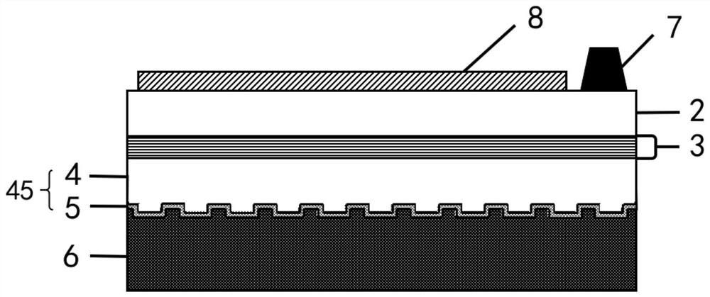
[0044] like figure 1 As shown, the present embodiment is a GaN-based resonant cavity light-emitting diode, which includes a supporting substrate 6, a high-contrast grating 45, an active region 3, and an N-type layer 2 that are stacked in sequence, and the N-type layer 2 is far away from the The end face of the active region is also provided with a first mirror 8 and an N electrode 7;

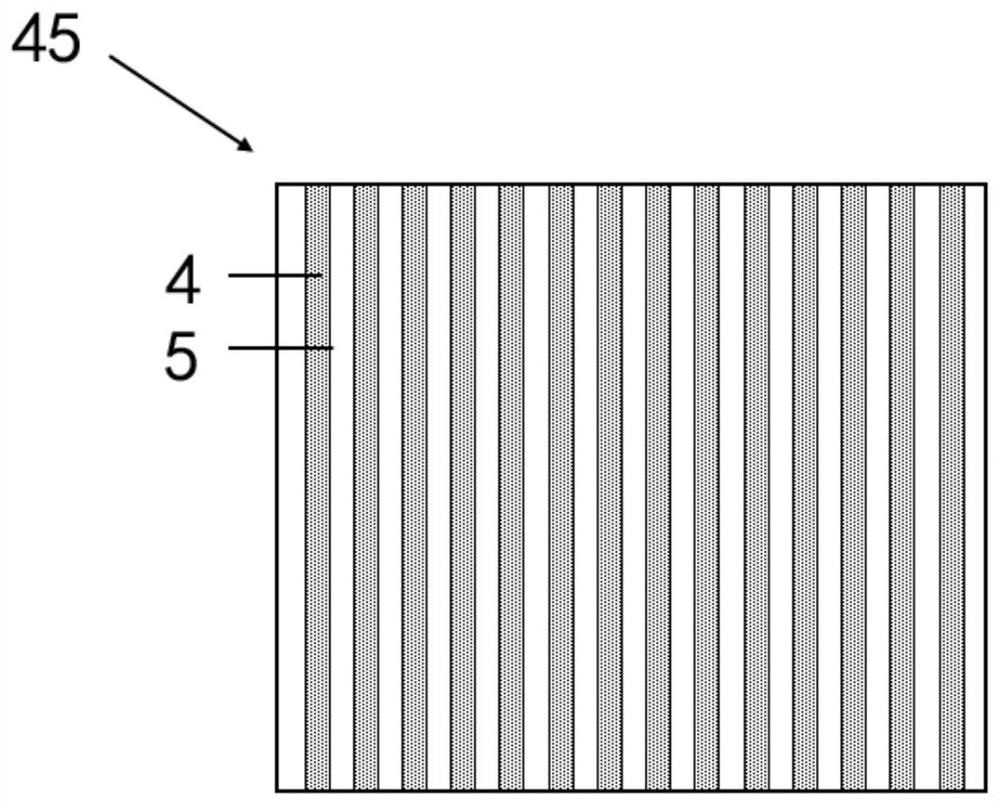
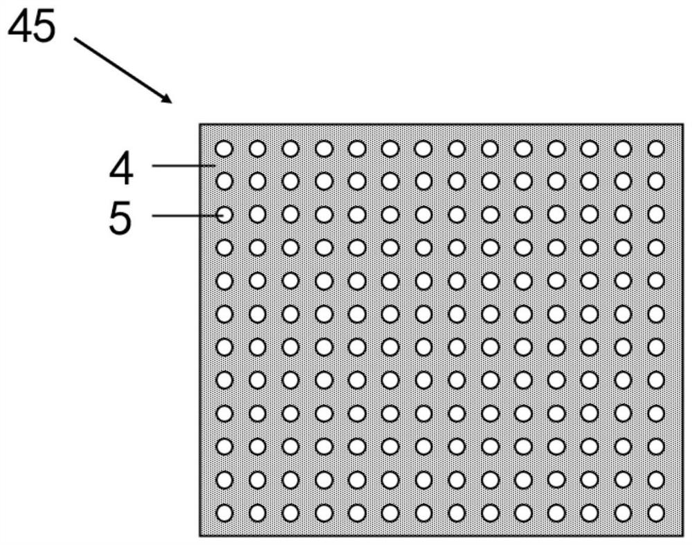
[0045]The high-contrast grating 45 is compose...


PUM

PropertyMeasurementUnit
depthaaaaaaaaaa

Abstract

The invention discloses a gallium nitride-based resonant cavity light-emitting diode and a preparation method thereof. The gallium-nitride-based resonant cavity light-emitting diode comprises a supporting substrate, a high-contrast grating, an active region, an N-type layer, and an N-type layer arranged in sequence. The end face of the layer away from the active area is also provided with a first mirror and an N electrode; wherein, the high-contrast grating is composed of a P-type layer and a transparent conductive layer, one end face of the P-type layer is attached to the active area, and the P-type layer The other end face of the P-type layer is etched to form a non-flat grating structure, and the transparent conductive layer is arranged on the gap and surface of the grating structure of the P-type layer; this scheme directly uses part of the P-type layer and the transparent conductive layer as the high-contrast grating structure to replace the traditional The bottom mirror structure of the device not only reduces the series resistance of the device, reduces the absorption loss, but also improves the quality of the output light, and the preparation process is simple, all the preparation processes are compatible with the standard semiconductor preparation process, and meet the needs of large-scale optoelectronic integration.

Description

technical field [0001] The invention relates to the technical field of semiconductor light-emitting, in particular to a gallium nitride-based resonant cavity light-emitting diode and a preparation method thereof, which are suitable for semiconductor resonant cavity devices of various wavelengths (visible light band, ultraviolet light band), including vertical cavity surface emission Lasers and Resonator Light Emitting Diodes. Background technique [0002] Semiconductor resonant cavity light-emitting diodes (Resonant Cavity Light Emitting Diode, RCLED) have a wide range of applications, including semiconductor lighting, backlight display, biomedical, optical communication and so on. It consists of top and bottom mirrors for optical feedback, and an active region sandwiched between them for providing outgoing photons. Broadband cavity mirrors with high reflectivity are a necessary condition for constructing high-quality factor resonant cavity devices. The bottom reflector us...

Claims


Application Information

Patent Timeline
Patent Type & Authority Patents(China)
IPC IPC(8): H01L33/10H01L33/46
CPCH01L33/10H01L33/105H01L33/46H01L33/465
Inventor 张保平徐欢梅洋杨帅应磊莹侯想罗荣煌卢文瑞陈锋钟梦洁刘熠新
Owner XIAMEN UNIV
Why Eureka
Try Eureka