Integrated substrate gap waveguide millimeter wave annular coupler based on multilayer packaging

A gap waveguide and integrated substrate technology, applied in the electrical field, can solve the problems of not meeting the design requirements of high-frequency circuits, mode conversion loss, and high processing costs, and achieve the effects of easy processing and integration, reduced transmission loss, and compact structure

Inactive Publication Date: 2021-09-28
BEIJING UNIV OF POSTS & TELECOMM
View PDF4 Cites 2 Cited by
  • Summary
  • Abstract
  • Description
  • Claims
  • Application Information

AI Technical Summary

Problems solved by technology

Traditional waveguide structures such as microstrip line structure, stripline structure or rectangular waveguide structure can no longer meet the design requirements of high frequency circuits due to the problems of radiation loss, surface wave, insertion loss, high processing cost and easy mode conversion loss. , so researchers have turned their attention to the gap waveguide structure that can be applied to the millimeter wave frequency band

Method used


Image

  • Integrated substrate gap waveguide millimeter wave annular coupler based on multilayer packaging
  • Integrated substrate gap waveguide millimeter wave annular coupler based on multilayer packaging
  • Integrated substrate gap waveguide millimeter wave annular coupler based on multilayer packaging

Examples


Embodiment

[0051] The above descriptions are only preferred embodiments of the present invention, and are not intended to limit the present invention. Any modifications, equivalent replacements, improvements, etc. made within the spirit and principles of the present invention shall be included in the present invention. within the scope of protection.

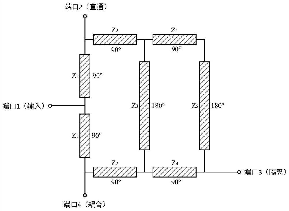
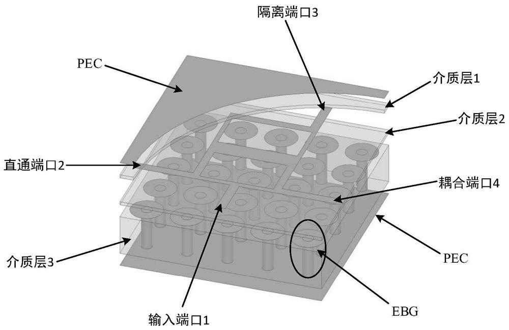
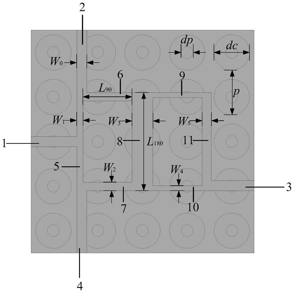
[0052] At present, experts and scholars in the field of radio frequency have begun to study millimeter wave devices. In order to meet the requirements of future communication systems, the present invention shows an embodiment of a millimeter wave ring coupler based on a multilayer package integrated substrate gap waveguide.

[0053] Among them, Rogers RT / duroid 5880 is selected for the gap layer of dielectric layer 1 and the middle layer of dielectric layer 2, the dielectric constant is 2.2, the thickness is 0.127mm, and the dielectric loss is 0.0009. The PMC layer of dielectric layer 3 is Rogers RO4350B, the dielectric constant is 3.48, an...


PUM

PropertyMeasurementUnit
thicknessaaaaaaaaaa
thicknessaaaaaaaaaa
widthaaaaaaaaaa

Abstract

The invention discloses an integrated substrate gap waveguide millimeter wave annular coupler based on multilayer packaging, which belongs to the electrical field, and is characterized in that three layers of media are constructed, the bottommost layer is a PMC layer of which the lower surface is coated with metal copper, a plurality of metal via holes are periodically arranged in the layer, the upper edge tightly abuts against a circular metal patch, and the lower edge is connected with the metal copper to form a mushroom-shaped EBG array; the middle layer is a layer of dielectric plate; the uppermost layer is a gap layer, the lower surface is printed with a hybrid ring coupling microstrip line, and the upper surface is coated with a layer of metal copper; the microstrip line comprises four sections of microstrip lines as ports, and seven sections of microstrip lines form a two-section hybrid ring; different ports are excited, and the bandwidth is enhanced to 50% through the two-section hybrid ring structure; and the metal copper on the uppermost layer and the mushroom type EBG array on the lowermost layer in the three layers of dielectric plates form a substrate gap waveguide, the working frequency band is distributed between 24 GHz and 40 GHz, and most of 5G millimeter wave frequency bands are covered. The antenna is low in transmission loss, compact in structure and easy to process and integrate.

Description

technical field [0001] The invention belongs to the electrical field, and relates to a passive radio frequency device, in particular to a millimeter-wave ring coupler based on a multilayer packaging integrated substrate gap waveguide. Background technique [0002] In recent years, people's demand for wireless communication has been increasing day by day, which has continuously promoted the development of communication technology. With the popularization of wireless communication equipment, low-frequency spectrum resources have become increasingly tight. The crowded spectrum has been unable to meet the high-speed, large-capacity and low latency requirements. [0003] With the development of 5G mobile communication systems, the entire mobile communication industry has begun to explore new frequency bands. Research on high-frequency frequency bands, especially millimeter wave frequency bands, has attracted more and more attention from researchers, experts and scholars. As an i...

Claims


Application Information

Patent Timeline
Patent Type & Authority Applications(China)
IPC IPC(8): H01P5/18
CPCH01P5/184
Inventor 吴永乐马润泽王卫民
Owner BEIJING UNIV OF POSTS & TELECOMM
Why Eureka
Try Eureka