In-situ tungsten deposition without using barrier layer
A technology of barrier layer and metal layer, which is applied in the direction of coating, metal material coating process, gaseous chemical plating, etc., can solve the problems of high resistivity and poor conduction of nucleation layer
- Summary
- Abstract
- Description
- Claims
- Application Information
AI Technical Summary
Problems solved by technology
Method used
Image
Examples
example
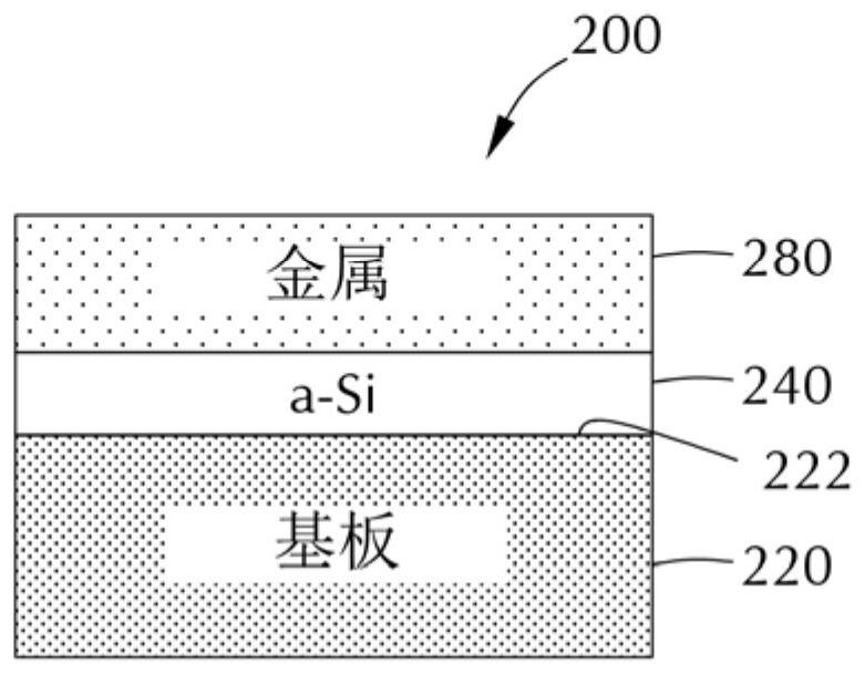
[0150] For each of the following examples, samples were prepared by depositing a tungsten layer on an amorphous tungsten layer. The amorphous tungsten layer is formed by converting the amorphous silicon layer.
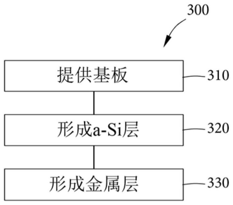
[0151] A nucleation layer including amorphous silicon (a-Si) is formed on the surface of the substrate by exposing the surface of the substrate to a nucleation precursor including disilane. The thickness of the nucleation layer is about to appointment within range. The surface of the substrate is substantially free of the barrier layer prior to exposure to the nucleation precursor. exposing the nucleation layer to WF at a partial pressure ranging from about 0.1 Torr to about 0.5 Torr 6 to transform the nucleation layer into a first metal layer comprising amorphous tungsten (a-W). Using WF by Atomic Layer Deposition 6 and H 2 A second metal layer is formed on the first metal layer.
example 1
[0153] Samples were prepared as indicated above. Some samples were processed "in situ" without air partition. Other samples were processed "ex situ" with air partition after formation of the nucleation layer but before formation of the first metal layer.
[0154] Samples prepared ex situ are shown in The resistivity of the lower pair of the second metal layer is about 30 μΩ·cm. Samples prepared ex situ are shown in The lower pair of the second metal layer has a resistivity of about 17 μΩ·cm.
[0155] Take pictures of the samples. Figure 11A An image of the in situ sample is shown in , while Figure 11B Images of ex situ samples are shown in . The darker layer in these images is the first metal layer. The images show that the first metal layer of the in situ processed sample has better film continuity compared to the ex situ processed sample.
[0156] Film adhesion tests were also performed on these samples. A piece of tape is brought into contact with the sample an...
example 2
[0158] Samples were also prepared on CVD OX and 1K OX substrates. CVD OX substrates are prepared by exposing a silicon substrate to a CVD process to deposit a silicon oxide layer. An aluminum oxide layer was deposited on silicon oxide and the substrate was spike annealed before further processing.
[0159] By thermally oxidizing silicon substrates in a furnace to form a thickness of approximately The silicon oxide layer was used to prepare the 1K OX substrate. An aluminum oxide layer is deposited on the silicon oxide layer. Substrates were not annealed prior to further processing.
[0160] The substrates were further processed to prepare the samples indicated above. Some samples were processed "in situ" without air partition. Other samples were processed "ex situ" with an air partition after forming the first metal layer but before forming the second metal layer.
[0161] Evaluate the sample for the second metal layer in the Resistivity, stress, resistance non-uniform...
PUM
 Abstract
Description
Claims
Application Information
 - R&D Engineer
- R&D Manager
- IP Professional
- Industry Leading Data Capabilities
- Powerful AI technology
- Patent DNA Extraction
Browse by: Latest US Patents, China's latest patents, Technical Efficacy Thesaurus, Application Domain, Technology Topic, Popular Technical Reports.
© 2024 PatSnap. All rights reserved.Legal|Privacy policy|Modern Slavery Act Transparency Statement|Sitemap|About US| Contact US: help@patsnap.com


