Check patentability & draft patents in minutes with Patsnap Eureka AI!

Self-aligned pattern process method

A process method and self-alignment technology, applied in electrical components, transistors, electrical solid devices, etc., can solve problems such as micro pattern size failure and structural collapse

Active Publication Date: 2021-10-19
CHANGXIN MEMORY TECH INC
View PDF5 Cites 0 Cited by
  • Summary
  • Abstract
  • Description
  • Claims
  • Application Information

AI Technical Summary

Problems solved by technology

[0004] However, in the process of forming micro-patterns in the target layer using self-aligned patterning technology, it is easy to cause the problem of size failure and structural collapse of micro-patterns as the line width shrinks.

Method used


Image

  • Self-aligned pattern process method
  • Self-aligned pattern process method
  • Self-aligned pattern process method

Examples


Embodiment Construction

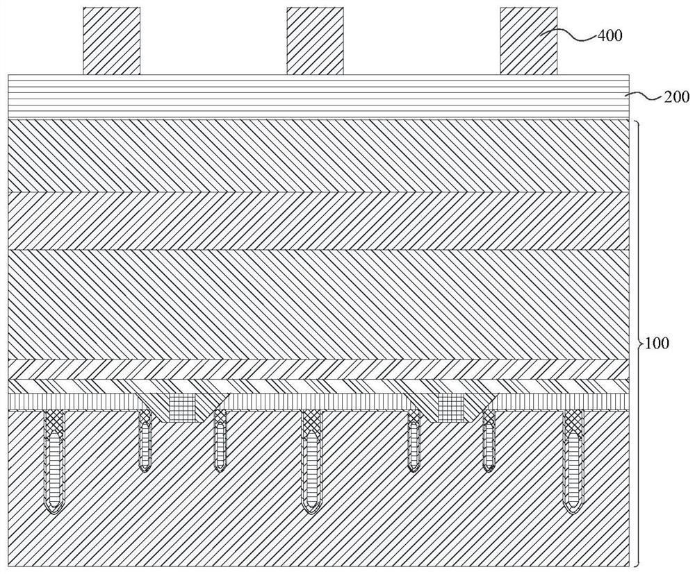
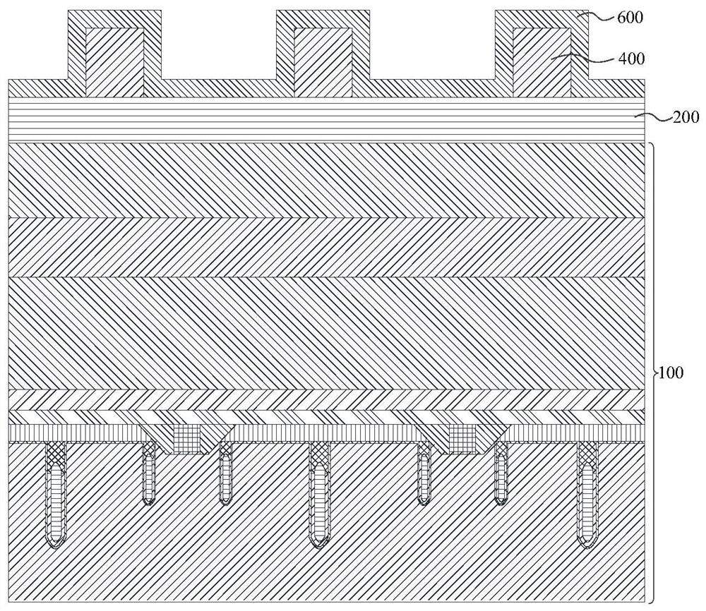
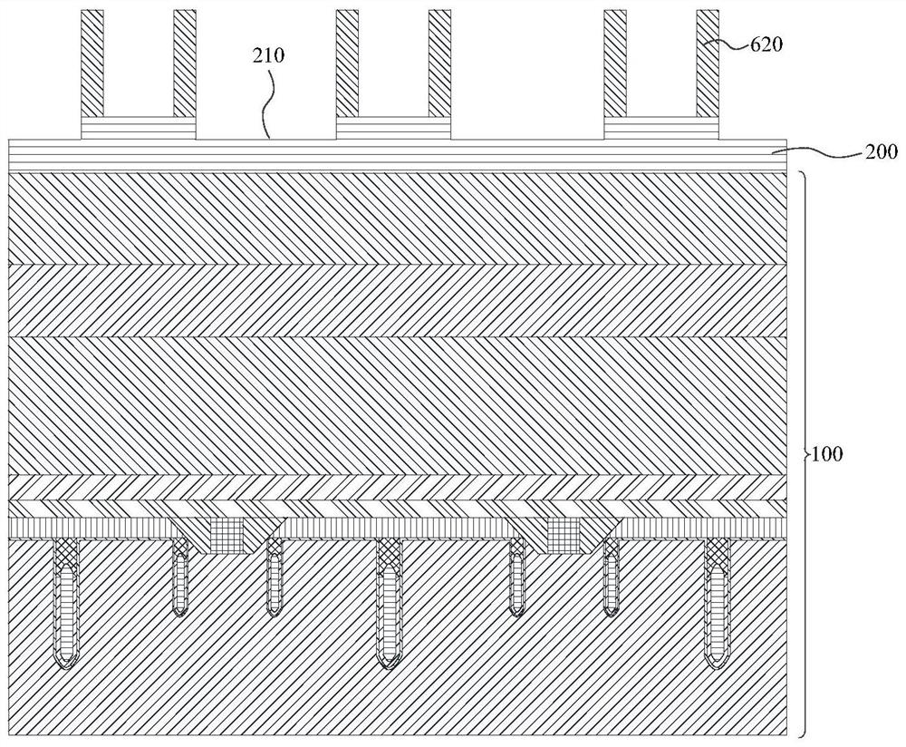
[0054] In related technologies, see Figure 1 to Figure 3 As shown, the self-aligned pattern process method includes the following steps: sequentially forming a stacked first hard mask layer 200, a sacrificial layer 400 and a photoresist layer 800 on the target layer 100, and patterning the photoresist layer 800; The patterned photoresist layer 800 is a mask, and part of the sacrificial layer 400 is removed to expose the first hard mask layer 200. The sacrificial layer 400 remaining on the first hard mask layer 200 forms a plurality of sacrificial patterns. forming a first sidewall material layer 600 on the mask layer 200 and the sacrificial pattern; The first sidewall material layer 600 on the top of the film layer 200, retaining the first sidewall material layer 600 on the sidewall of each sacrificial pattern; removing the sacrificial layer 400 in each sacrificial pattern, exposing the first hard mask in each sacrificial pattern layer 200 to form a plurality of first sidewa...


PUM


Abstract

The invention provides a self-aligned pattern process method, relates to the technical field of semiconductor manufacturing, and aims at solving the problems of size failure and structure collapse easily caused in a micro pattern manufacturing process. The process method comprises the following steps of: forming a first hard mask layer, a patterned sacrificial layer and a second hard mask layer on a target layer, forming first sacrificial patterns, and forming a pit in the side wall of the second hard mask layer in the first sacrificial patterns; forming a first spacer material layer on the first hard mask layer and each first sacrificial pattern, the first spacer material layer being provided with a spacer extension part embedded in the pit; removing part of the first spacer material layer, and retaining the first spacer material layer on the side wall of each first sacrificial pattern; removing the sacrificial layer in each first sacrificial pattern to form a plurality of first spacer patterns; and transferring the first spacer patterns to form a target pattern on a target layer. The method is used for solving the problems of size failure and structure collapse caused when a micro pattern is manufactured.

Description

technical field [0001] The invention relates to the technical field of semiconductor manufacturing, in particular to a self-aligned pattern process method. Background technique [0002] In the manufacturing process of semiconductor devices, the manufacture of some microstructures requires the use of photolithography and etching to form tiny patterns with precise dimensions in target layers such as semiconductor substrates or dielectric layers formed on the substrates. [0003] For this purpose, in conventional semiconductor technology, a mask layer is formed over the target layer in order to first form these minute patterns in the mask layer and then transfer the pattern to the target layer. With the complication of integrated circuits, the size of these tiny patterns continues to decrease, and self-aligned double pattern technology (Self-Aligned Double Pattern, SADP) or self-aligned quadruple pattern technology (Self-Aligned Quadruple Pattern, SAQP ) is one of the key tech...

Claims


Application Information

Patent Timeline
Patent Type & Authority Applications(China)
IPC IPC(8): H01L21/027H01L21/033H01L27/108H10B12/00
CPCH01L21/0332H01L21/0337H01L21/0274H10B12/01
Inventor 金星李冉李昇孙正庆
Owner CHANGXIN MEMORY TECH INC
Features
  • R&D
  • Intellectual Property
  • Life Sciences
  • Materials
  • Tech Scout
  • Unparalleled Data Quality
  • Higher Quality Content
  • 60% Fewer Hallucinations
Learn More