Negative electrode material, electrochemical device, and electronic device
A negative electrode material, electrochemical technology, applied in the field of electrochemical devices and electronic devices, can solve the problems of accelerating material attenuation and failure, accelerating carbon layer peeling, etc., to achieve the goal of reducing energy barrier, increasing bond length, and improving electron and ion conduction Effect
- Summary
- Abstract
- Description
- Claims
- Application Information
AI Technical Summary
Problems solved by technology
Method used
Image
Examples
preparation example Construction
[0039] Second, the preparation method of silicon-based composite
[0040] The present application also provides a method for preparing a silicon-based composite, which includes the following steps:
[0041] Step A: Mix the gas phase first mixture (Si and SiOx molar ratio is 1:1, 0.5<x<1.5) with the gas phase dopant element source (germanium dioxide or boric acid) and deposit on the substrate to obtain a silicon-based composite a precursor, wherein the gas phase first mixture comprises silicon oxide;
[0042] Step B: cooling the silicon-based composite precursor to obtain the silicon-based composite.
[0043] According to some embodiments of the present application, the preparation of the first mixture in the gas phase includes heat-treating the first mixture, wherein the first mixture includes silicon oxide.
[0044] According to some embodiments of the present application, the preparation of the gas-phase doping element source includes heating the doping element source.
...
Embodiment 1
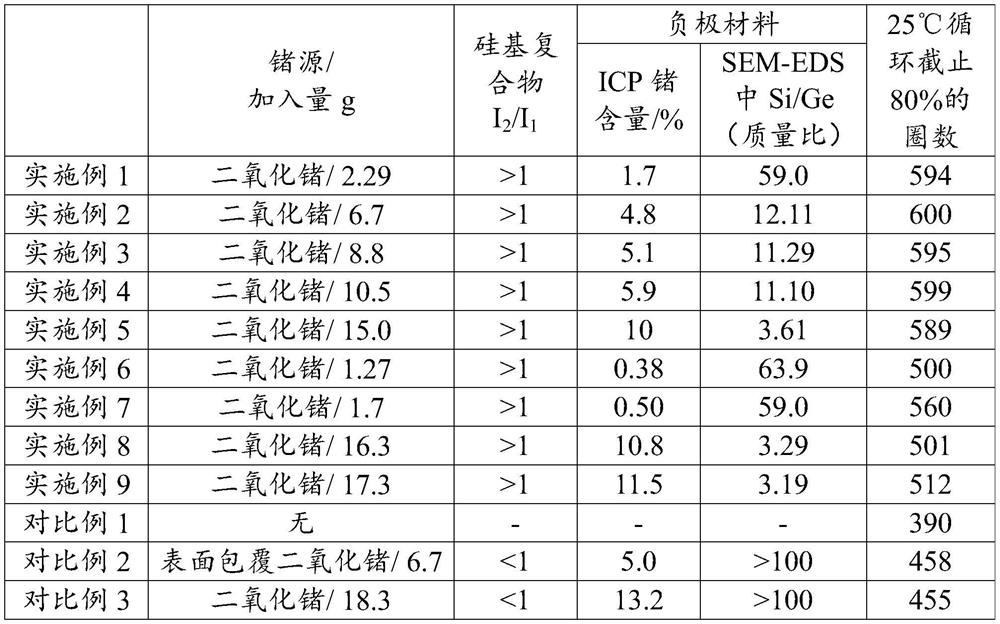
[0134] The comparison between Example 1 and Comparative Example 2 shows that bulk phase doping of SiOx with germanium can improve the ionic and electronic conductivity of the entire material, while surface doping only improves the properties of the material surface, and the cycle of bulk phase doping is better than surface doping.
[0135] The comparison between Example 1 and Comparative Example 3 shows that: Comparative Example 3 is a mixture of germanium and silicon oxide, and is not bulk phase doped, and the content of germanium is higher than 10%, and the cycle performance of Comparative Example 3 is poor.
[0136] In Table 2, the amount of metal silicon powder added in the preparation process of the negative electrode material was 28g, the amount of fumed silica powder added was 60g, and amorphous carbon was used for CVD coating of the surface carbon material.
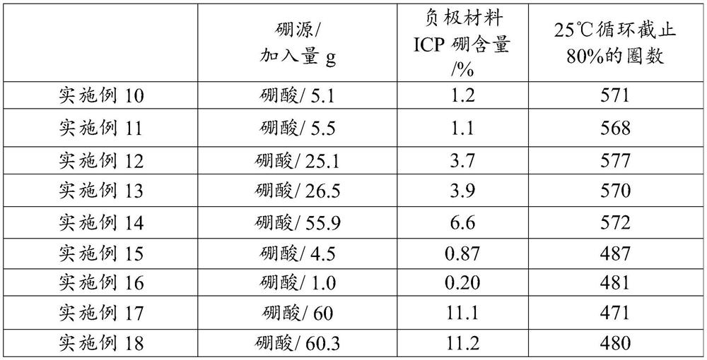
[0137] Wherein each parameter value of the negative electrode material of embodiment 10 to embodiment 18 is as f...
Embodiment 2
[0150] Other parameter values of the negative electrode material of embodiment 2, embodiment 19 to embodiment 27 are as follows:
[0151] Dv50 are 3.2μm, 3.2μm, 3.2μm, 3.2μm, 3.2μm, 3.2μm, 3.2μm, 5.2μm, 2.6μm, 5.5μm;
[0152] Dv90 are 6.9μm, 6.8μm, 6.9μm, 6.8μm, 6.7μm, 6.9μm, 6.8μm, 8.0μm, 6.9μm, 8.0μm;
[0153] Dv99 are 9.5μm, 9.4μm, 9.3μm, 9.4μm, 9.5μm, 9.5μm, 9.4μm, 12.0μm, 9.3μm, 12.01μm;
[0154] BET is 2.9m respectively 2 / g, 2.9m 2 / g, 2.8m 2 / g, 2.7m 2 / g, 2.8m 2 / g, 2.7m 2 / g, 2.9m 2 / g, 2.0m 2 / g, 4.4m 2 / g, 3.3m 2 / g;
[0155] The values of relational expression (1) are 2.01, 1.97, 1.81, 1.97, 2.14, 2.01, 1.97, 3.84, 1.81, 3.85;
[0156] The values of relational expression (2) are 3.99, 3.98, 3.89, 3.78, 3.87, 3.79, 3.98, 3.21, 5.49, 4.52, respectively.
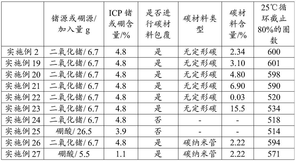
[0157] table 3
[0158]
[0159] The comparison of Example 2 and Example 19 to Example 25 shows that the content of carbon needs to be between 0.1% and 10%. If the content is lower than 0.1%,...
PUM
| Property | Measurement | Unit |
|---|---|---|
| particle diameter | aaaaa | aaaaa |
| specific surface area | aaaaa | aaaaa |
| particle diameter | aaaaa | aaaaa |
Abstract
Description
Claims
Application Information


