Layered wave-absorbing material and preparation method thereof

A wave-absorbing material and layered technology, which is applied in the field of layered wave-absorbing materials and their preparation, can solve the problems affecting the wave-absorbing performance of materials, the difficulty of precise control of shape and structure, and the difficulty of precise control of structure, so as to achieve reliable quality, Improved impedance matching performance and electromagnetic wave attenuation performance, and high processing efficiency

Active Publication Date: 2021-10-29
SHENZHEN GRADUATE SCHOOL TSINGHUA UNIV
View PDF5 Cites 0 Cited by
  • Summary
  • Abstract
  • Description
  • Claims
  • Application Information

AI Technical Summary

Problems solved by technology

[0003] At present, most of the preparation of microwave-absorbing materials involves complex chemical methods and complex process steps, and the shape and structure are difficult to precisely control, or extremely complex equipment and methods are required to precisely control the structure and composition to meet impedance matching and electromagnetic wave attenuation. Require
In addition, the thickness of the currently prepared absorbing materials is basically at the millimeter level or even thicker to meet the requirements of absorbing performance. It is still a huge challenge to prepare extremely thin and high-performance absorbing materials.
Moreover, most of the conductive polymer absorbing materials made of nanomaterials and polymers are usually a mixture of the two, so the structure is difficult to precisely control, and this defect also greatly affects the absorbing properties of the material. wave performance

Method used


Image

  • Layered wave-absorbing material and preparation method thereof
  • Layered wave-absorbing material and preparation method thereof
  • Layered wave-absorbing material and preparation method thereof

Examples


preparation example Construction

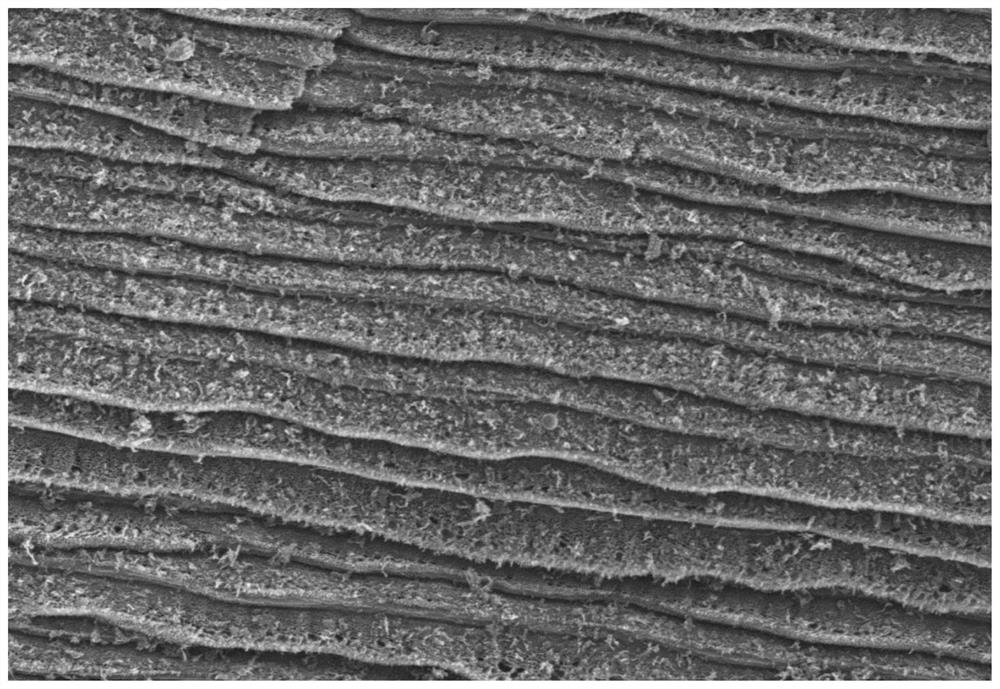
[0017] A method for preparing a layered wave-absorbing material, the layered wave-absorbing material comprising a base layer, a lossy layer formed on the base layer, and a polymer carbonized layer formed on the lossy layer; the preparation method Include the following steps:

[0018] (1) Laser carbonizing the polymer film to form carbides to form the base layer, and coating the base layer with a mixture solution of metal salts;

[0019] (2) laser treating the mixture solution of the metal salt to form the lossy layer, and coating a polymer solution on the lossy layer;

[0020] (3) laser processing the high molecular polymer solution to form the high molecular carbonized layer;

[0021] (4) If the lossy layer is greater than 1 layer and the polymerized carbonized layer is greater than 1 layer, repeat steps (2) and (3) to form the lossy layer and the polymerized carbonized layer on the base layer an overlay of alternating layers;

[0022] (5) Annealing the material obtained a...

Embodiment 1

[0036] The preparation method of layered wave-absorbing material comprises the following steps:

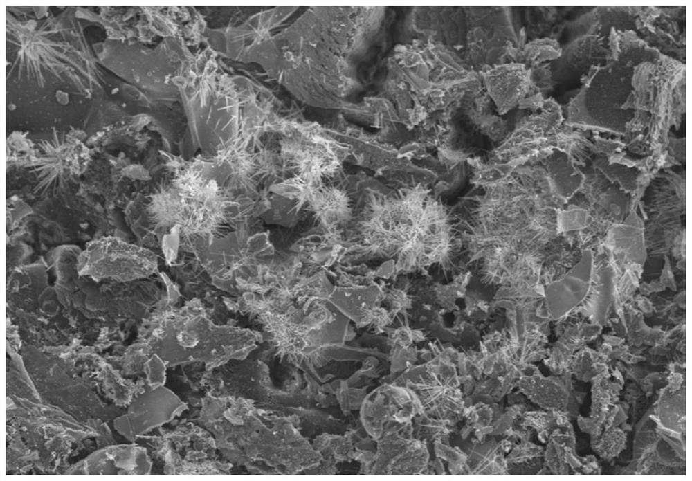
[0037] 1. Making the base layer: The polymer film used to make the base layer is a PI film with a thickness of 50 μm. Before use, it is washed repeatedly with deionized water and ethanol for 3-5 times, and then dried at a constant temperature of 60°C for 30 minutes. Then move the cleaned and dried PI film into a square hollow container that can provide an inert gas atmosphere for laser processing, wherein the inert gas inlet and outlet rates of the inert gas inlet and outlet on both sides of the hollow container The inert gas here is nitrogen at 10ml / min. The PI film can be processed by a pulsed laser with a high repetition rate. It can be processed once or twice with the same or different processing accuracy. In this example, the first rough processing and the second fine processing are used. Secondary processing technology to precisely control the micro-nano porous structure. ...

Embodiment 2

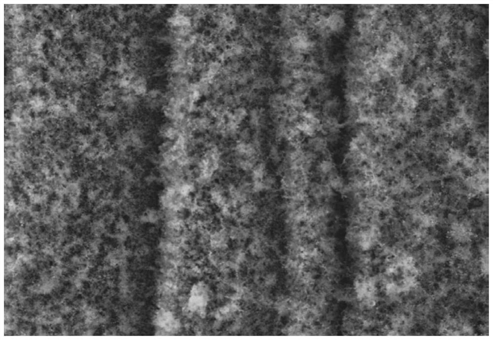
[0044] The difference from Example 1 is that the laser processing parameters in step 1 are different. In this embodiment, the PI film is processed by one laser processing, and the parameters are set as follows: laser power is 4w, repetition frequency is 800KHz, and defocus is 10μm , The scanning speed is 50mm / s, and the scanning distance is 10μm. The SEM figure of the base layer that this embodiment obtains is as Figure 6 shown.

[0045] The thickness and absorbing performance of the layered absorbing material prepared by the present invention can be determined by the type of laser, the working parameter setting of the laser, the type of polymer film, the mixture solution of metal salt, the polymer solution, and the temperature and time of annealing, etc. parameter adjustment.


PUM

PropertyMeasurementUnit
diameteraaaaaaaaaa
thicknessaaaaaaaaaa

Abstract

The invention discloses a layered wave-absorbing material and a preparation method thereof. The preparation method comprises the steps of (1) carrying out laser carbonization on a polymeric membrane to form a carbide to form a substrate layer, and coating the substrate layer with a mixture solution of metal salt; (2) performing laser treatment on the mixture solution of the metal salt to form a loss layer, and coating the loss layer with a high-molecular polymer solution; (3) performing laser treatment on the high-molecular polymer solution to form a high-molecular carbonized layer; (4) if the loss layer is more than one and the high-molecular carbonized layer is more than one, repeating the step (2) and the step (3) to form a stacked layer formed by alternately stacking the loss layer and the high-molecular carbonized layer on the substrate layer; and (5) carrying out annealing treatment on the material obtained in the steps (1)-(4) to obtain the layered wave-absorbing material. The layered wave-absorbing material prepared by the invention has the advantages of simple preparation method, small thickness, quick batch production, adjustable wave-absorbing performance, good wave-absorbing effect and the like.

Description

technical field [0001] The invention relates to the technical field of preparation of wave-absorbing materials, in particular to a layered wave-absorbing material and a preparation method thereof. Background technique [0002] Science and technology are developing and advancing at a rapid pace. At the same time, the emergence of various emerging devices has also brought about increasingly serious electromagnetic pollution problems. Communication facilities such as artificial satellites and radars have brought great convenience to our lives, but they have also brought huge risks. Unfavorable electromagnetic wave pollution is causing more and more inconvenience to human life. Especially in the fields of electronic communication, public transportation and military affairs, the efficient absorption of unfavorable electromagnetic waves is of great significance. Therefore, the research and preparation of high-efficiency absorbing materials have always been concerned by people, a...

Claims


Application Information

Patent Timeline
Patent Type & Authority Applications(China)
IPC IPC(8): B32B27/00B32B27/06B32B27/08B32B27/28B32B27/36B32B9/00B32B9/04B32B33/00
CPCB32B27/06B32B27/00B32B27/281B32B27/36B32B9/00B32B9/045B32B27/08B32B33/00
Inventor 杨诚刘明杰王方成高强苏陟
Owner SHENZHEN GRADUATE SCHOOL TSINGHUA UNIV
Why Eureka
Try Eureka