Silicon carbide crystal growth device and method

A technology of crystal growth and silicon carbide, applied in crystal growth, chemical instruments and methods, single crystal growth, etc., can solve the problem of unavoidable carbon-wrapped SF and BPD, and achieve simple structure, convenient setting, and good quality

Active Publication Date: 2021-11-09
FUJIAN NORSTEL MATERIAL TECH CO LTD
View PDF11 Cites 1 Cited by
  • Summary
  • Abstract
  • Description
  • Claims
  • Application Information

AI Technical Summary

Problems solved by technology

These problems make it impossible to avoid the three defects of carbon wrapping, SF and BPD by using silicon carbide crystals grown on flat surfaces.

Method used


Image

  • Silicon carbide crystal growth device and method

Examples


Embodiment Construction

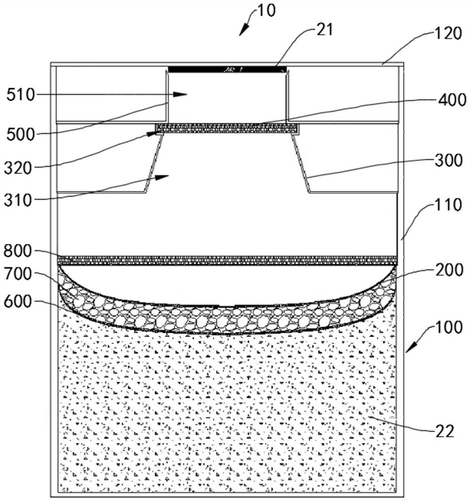
[0055] In order to make the purposes, technical solutions and advantages of the embodiments of the present invention clearer, the technical solutions in the embodiments of the present invention will be clearly and completely described below with reference to the accompanying drawings in the embodiments of the present invention. Obviously, the described embodiments These are some embodiments of the present invention, but not all embodiments. The components of the embodiments of the invention generally described and illustrated in the drawings herein may be arranged and designed in a variety of different configurations.

[0056] Thus, the following detailed description of the embodiments of the invention provided in the accompanying drawings is not intended to limit the scope of the invention as claimed, but is merely representative of selected embodiments of the invention. Based on the embodiments of the present invention, all other embodiments obtained by those of ordinary ski...


PUM


Abstract

The invention relates to the technical field of crystal growth, and concretely relates to a silicon carbide crystal growth device and method. The silicon carbide crystal growth device comprises a crucible and a net-shaped piece; the net-shaped piece is arranged in a crucible body of the crucible, and the periphery of the net-shaped piece abuts against the inner wall of the crucible body; the net-shaped piece is in a concave shape towards the bottom of the crucible body; and the bottom of the crucible is configured to be used for containing raw material powder, the net-shaped piece is configured to be attached to and cover the raw material powder, and the surface, facing the top face of the crucible body, of the raw material powder is provided with a concave shape matched with the net-shaped piece. The thermal field can be effectively utilized by changing the concave-convex degree of the charge level, so that the internal stress of the crystal is reduced, the nitrogen doping is more uniform, the occurrence of SF is solved from two aspects, and the density of BPD is reduced as much as possible.

Description

technical field [0001] The present invention relates to the technical field of crystal growth, in particular, to a silicon carbide crystal growth device and a crystal growth method. Background technique [0002] During the growth process of the silicon carbide crystal in the prior art, as the thickness of the produced crystal increases, the distance from the flat material surface to the crystal surface changes, and the thermal field is no longer suitable. [0003] Due to the large consumption of silicon in the middle and later stages of growth, the proportion of carbon will be higher. At this time, the unsuitable thermal field will cause carbonization of the material surface, inducing the appearance of carbon wrapping and the generation of stacking fault (SF). At the same time, due to the mismatch between the convexity of the crystal surface and the flat material surface, the crystal grown using the flat material surface generates axial stress in the later stage, and there a...

Claims


Application Information

Patent Timeline
Patent Type & Authority Applications(China)
IPC IPC(8): C30B11/00C30B29/36
CPCC30B11/002C30B29/36
Inventor 王睿仑张洁廖弘基杨树
Owner FUJIAN NORSTEL MATERIAL TECH CO LTD
Why Eureka
Try Eureka