Preparation method of light-emitting diode epitaxial wafer with p-type composite layer

A technology of light-emitting diodes and composite layers, which is applied to semiconductor devices, electrical components, circuits, etc., can solve the problems of unsatisfactory luminous efficiency of light-emitting diodes and many defects in the p-type GaN layer, and achieve improved luminous efficiency, improved luminous uniformity, The effect of improving the uniformity of light emission

Active Publication Date: 2021-11-12
HC SEMITEK ZHEJIANG CO LTD
View PDF3 Cites 2 Cited by
  • Summary
  • Abstract
  • Description
  • Claims
  • Application Information

AI Technical Summary

Problems solved by technology

However, the number of holes that the p-type GaN layer can provide is limited. If the p-type GaN layer is heavily doped with Mg to increase the number of holes, it will cause too many defects, and when there are too many Mg elements, it is easy to cause p-type The uneven doping of Mg in the GaN layer leads to the problem of many defects in the p-type GaN layer, which leads to the unsatisfactory luminous efficiency of the final light-emitting diode.

Method used


Image

  • Preparation method of light-emitting diode epitaxial wafer with p-type composite layer
  • Preparation method of light-emitting diode epitaxial wafer with p-type composite layer
  • Preparation method of light-emitting diode epitaxial wafer with p-type composite layer

Examples


Embodiment Construction

[0026] In order to make the purpose, technical solution and advantages of the present invention clearer, the embodiments of the present disclosure will be further described in detail below in conjunction with the accompanying drawings.

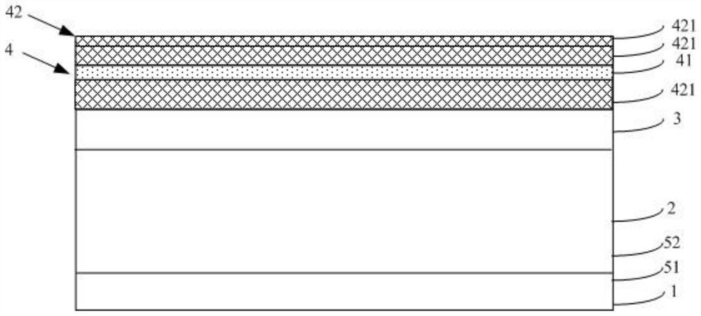
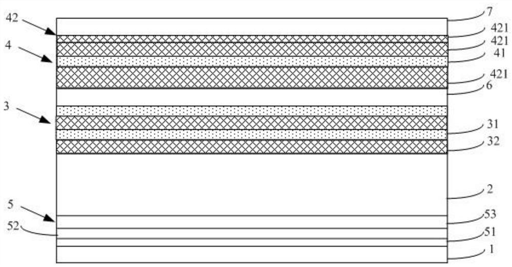
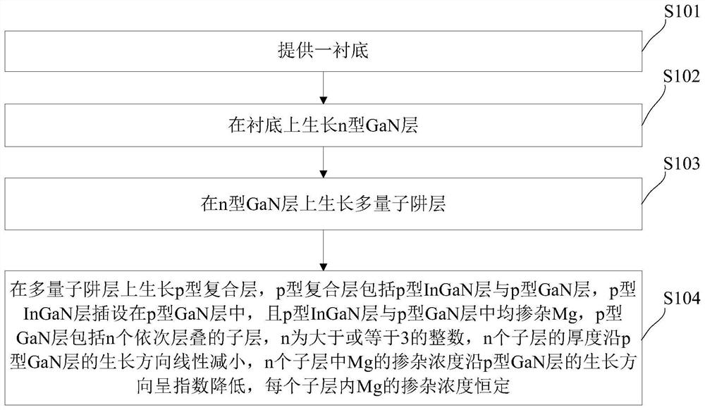
[0027] figure 1 It is a schematic structural diagram of a light-emitting diode epitaxial wafer with a p-type composite layer provided by an embodiment of the present disclosure. Refer to figure 1 It can be seen that the embodiment of the present disclosure provides a light emitting diode epitaxial wafer with a p-type composite layer, and the light emitting diode epitaxial wafer with a p-type composite layer includes an n-type GaN layer 2, a multi-quantum well layer 3 and a p-type composite layer 4 , the p-type composite layer 4 includes a p-type InGaN layer 41 and a p-type GaN layer 42, the p-type InGaN layer 41 is inserted in the p-type GaN layer 42, and both the p-type InGaN layer 41 and the p-type GaN layer 42 are doped Mg, the p-type GaN ...


PUM

PropertyMeasurementUnit
thicknessaaaaaaaaaa
thicknessaaaaaaaaaa
thicknessaaaaaaaaaa

Abstract

The invention discloses a preparation method of a light-emitting diode epitaxial wafer with a p-type composite layer, and belongs to the field of light-emitting diode manufacturing. The p-type composite layer is grown on a multi-quantum well layer, the p-type composite layer comprises a p-type InGaN layer and a p-type GaN layer, the In element has the effect of reducing the activation energy of Mg, and the activation rate of Mg in the p-type InGaN layer and the p-type GaN layer can be improved so as to improve the number of holes. The p-type InGaN layer is inserted in the p-type GaN layer, and the p-type InGaN layer can be used as a low-barrier region, stores part of holes and expands the holes, so that the holes can enter the multi-quantum well layer more uniformly, and the light emitting uniformity of the light emitting diode is improved. The light-emitting efficiency and the light-emitting uniformity of the light-emitting diode can be improved.

Description

technical field [0001] The invention relates to the field of light-emitting diode production, in particular to a method for preparing a light-emitting diode epitaxial wafer with a p-type composite layer. Background technique [0002] A light emitting diode is a semiconductor electronic component that emits light. As an efficient, environmentally friendly and green new solid-state lighting source, it is being rapidly and widely used, such as traffic lights, car interior and exterior lights, urban landscape lighting, mobile phone backlight, etc. Improving the luminous efficiency of chips is the goal that LEDs are constantly pursuing. [0003] The light-emitting diode epitaxial wafer is the basic structure for preparing light-emitting diodes. The light-emitting diode epitaxial wafer includes at least a substrate and an n-type GaN layer on the substrate, a multi-quantum well layer and a p-type GaN layer. The p-type GaN layer is usually doped with Mg to increase the number of ho...

Claims


Application Information

Patent Timeline
Patent Type & Authority Applications(China)
IPC IPC(8): H01L33/32H01L33/06H01L33/00
CPCH01L33/325H01L33/0066H01L33/06H01L33/0075
Inventor 王群郭志琰王江波葛永晖董彬忠李鹏
Owner HC SEMITEK ZHEJIANG CO LTD
Why Eureka
Try Eureka