
Optical logic element for photoelectric digital logic operation and its logic operation method

A digital logic and optical logic technology, applied in the field of optical logic components, can solve problems such as low parameter scale, error, and system modulation rate limitation, and achieve the effect of large calculation scale, high modulation rate, and high unit energy consumption calculation performance

Active Publication Date: 2022-03-11
TSINGHUA UNIV
View PDF6 Cites 0 Cited by
  • Summary
  • Abstract
  • Description
  • Claims
  • Application Information

AI Technical Summary

Problems solved by technology

[0003] The optoelectronic digital logic operation chip is an important component to realize optoelectronic intelligent computing. At present, there are many ways to realize the optical digital logic gate: the optical digital logic gate can be realized by non-linear devices such as semiconductor optical amplifiers, periodically poled lithium niobate waveguides, and electroabsorption modulators. Its unit calculation energy consumption, noise and other performance are not ideal, and the integration potential is limited; in terms of integrated optical computing, the representative work in the world mainly includes matrix numerical calculation based on silicon photonics optical interference network array, optical phase change material array Realize the integration of storage and calculation, etc. Similar work has realized some simple optical calculations, but the current silicon photonics scheme has problems such as low parameter scale and relatively simple model structure; the optoelectronic Fourier domain convolutional neural network based on space optics has realized High-throughput optical computing, but the system modulation rate is limited, and errors are difficult to correct
In related technologies, there is a lack of a logic operation device that can perform large-scale operations and has a high modulation rate, which needs to be solved urgently

Method used


Image

  • Optical logic element for photoelectric digital logic operation and its logic operation method
  • Optical logic element for photoelectric digital logic operation and its logic operation method
  • Optical logic element for photoelectric digital logic operation and its logic operation method

Examples


Embodiment Construction

[0025] Embodiments of the present application are described in detail below, examples of which are shown in the drawings, wherein the same or similar reference numerals denote the same or similar elements or elements having the same or similar functions throughout. The embodiments described below by referring to the figures are exemplary, and are intended to explain the present application, and should not be construed as limiting the present application.

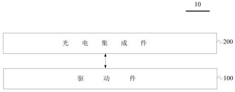
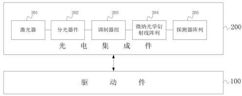
[0026] The following describes the optical logic element of the optical digital logic operation and the logic operation method of the embodiment of the present application with reference to the accompanying drawings. In view of the lack of a logic operation device capable of large-scale operations and high modulation rate mentioned in the background technology center mentioned above, this application provides an optical logic element for photoelectric digital logic operation and its logic operation method. The component dete...


PUM


Abstract

The present application relates to the technical field of optical logic elements, in particular to an optical logic element for optoelectronic digital logic operations and a logic operation method thereof, wherein the element includes: a drive element for providing a drive for an optoelectronic integrated element to generate an optoelectronic integrated element capable of Identify the digital modulation information and read the electrical signal output by the optoelectronic integrated part; the optoelectronic integrated part is used to use the coherent optical signal to carry the digital modulation information input by the drive part, and digitally carry out the coherent optical signal in the preset optical diffraction neural network The logic operation is to obtain the operation result, and generate the electric signal based on the digital logic mapping relationship, and output the operation result after reading the electric signal by the driver. The embodiment of the present application has higher computing performance per unit energy consumption, and different dedicated logic operations can be reconfigured and designed in batches, with large operation scale and high modulation rate.

Description

technical field [0001] The present application relates to the technical field of optical logic elements, in particular to an optical logic element for photoelectric digital logic operation and a logic operation method thereof. Background technique [0002] In the era of the new data-driven industrial revolution, computing power is the primary productive force. With the development of artificial intelligence technology, the corresponding artificial intelligence algorithms are becoming more and more complex. At present, the density and size of devices on traditional micro-nano electronic chips have approached physical limits, and power consumption and computing power are also facing bottlenecks. Photoelectric computing makes full use of the dual advantages of light in computing power and energy consumption, and has the potential to solve the computing power and power consumption bottlenecks currently faced by large-scale computing. Optoelectronics smart chips can bring more t...

Claims


Application Information

Patent Timeline
Patent Type & Authority Patents(China)
IPC IPC(8): H04B10/516H04B10/61
CPCH04B10/516H04B10/61G02F3/00G06N3/02G06N3/067G02F1/212G06N3/0675G06N3/045G06N3/044G06N3/048G06N3/04G06N3/08H04B10/556
Inventor 戴琼海郑纪元邓辰辰吴嘉敏
Owner TSINGHUA UNIV
Learn More