Lateral variable doping terminal structure and design method thereof

A terminal structure and design method technology, applied in CAD circuit design, electrical components, circuits, etc., can solve problems such as breakdown voltage reduction, charge sensitivity, and reliability impact of VLD terminals, so as to reduce impact and improve device withstand voltage Effect

Active Publication Date: 2021-11-16
UNIV OF ELECTRONICS SCI & TECH OF CHINA +1
View PDF8 Cites 2 Cited by
  • Summary
  • Abstract
  • Description
  • Claims
  • Application Information

AI Technical Summary

Problems solved by technology

[0003] However, the VLD terminal still has a disadvantage, which is specifically reflected in its sensitivity to charges. The charges here not only refer to the charges introduced by impurities in the VLD region, but also include trap charges, fixed charges, and movable charges.
In engineering applications, trap charges, fixed charges, and movable charges affect the reliability of VLD terminals, and the breakdown voltage decreases during reverse withstand voltage, which limits the application of VLD terminals.

Method used


Image

  • Lateral variable doping terminal structure and design method thereof
  • Lateral variable doping terminal structure and design method thereof
  • Lateral variable doping terminal structure and design method thereof

Examples


Embodiment 1

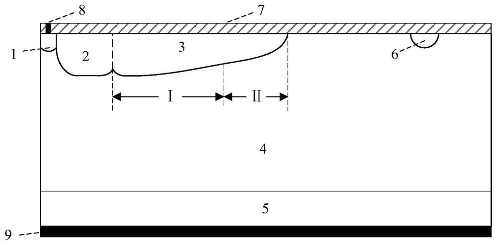
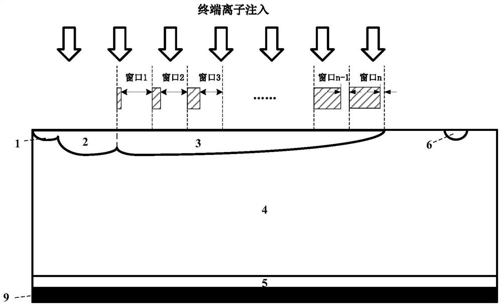
[0034] A laterally variable doping terminal structure, characterized in that it includes a passivation layer 7, a lightly doped first-type conductivity type drift region 4, and an anode region from the surface to the bottom, and the upper part of the interior includes a medium doping layer from left to right. The second conductivity type main junction region 1, the moderately doped second conductivity type transition region 2, the moderately doped second conductivity type segmented linear VLD termination region 3 and the heavily doped first conductivity type floating stop ring 6;

[0035] The anode region includes a heavily doped first conductivity type substrate 5 and an anode metal 9 below the heavily doped first conductivity type substrate 5, the heavily doped first conductivity type substrate 5 and the anode metal 9 form an ohmic contact, The anode metal 9 is connected to the external circuit; the main junction metal lead 8 is above the main junction region 1 of the medium-...

Embodiment 2

[0044] The difference between this embodiment and Embodiment 1 is that: the design method of the moderately doped second conductivity type piecewise linear VLD terminal region 3 is:

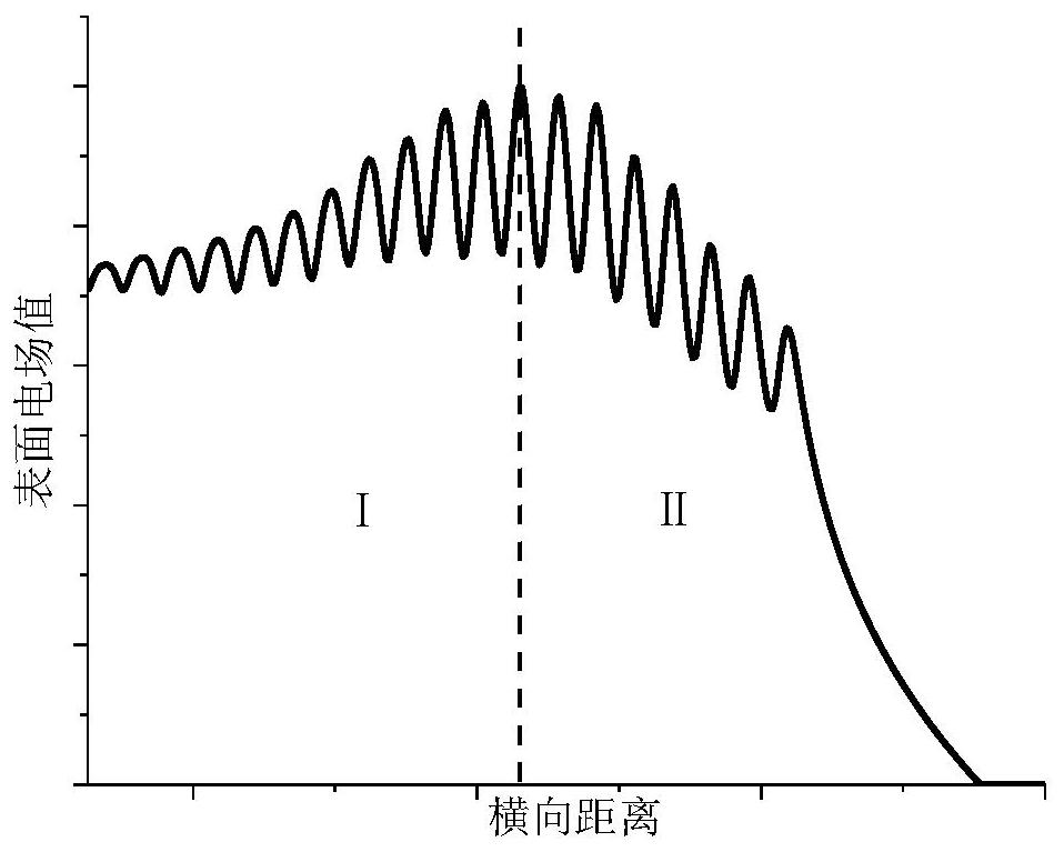
[0045] (1) First, the moderately doped second conductivity type piecewise linear VLD terminal region 3 is designed as a region where the impurity concentration decreases linearly from the main junction to the terminal end, and the surface electric field distribution is obtained through device simulation, and then the distance from the surface is selected. The implantation window closest to the electric field peak position is used as the turning point of the two-stage impurity concentration distribution region;

[0046] (2) The side near the main junction of the turning point is area I, and the side of the turning point close to the edge of the chip is area II, such as Figure 5 As shown, on the basis of the one-stage linear distribution, the window size at the turning point is controlled to be co...

Embodiment 3

[0048] This embodiment combines Embodiment 1 and Embodiment 2. The difference between this embodiment and Embodiment 1 is that the design method of the moderately doped second conductivity type segmented linear VLD terminal region 3 is as follows:

[0049] (1) First, the moderately doped second conductivity type piecewise linear VLD terminal region 3 is designed as a region where the impurity concentration decreases linearly from the main junction to the terminal end, and the surface electric field distribution is obtained through device simulation, and then the distance from the surface is selected. The implantation window closest to the electric field peak position is used as the turning point of the two-stage impurity concentration distribution region;

[0050] (2) The side near the main junction of the turning point is area I, and the side of the turning point close to the edge of the chip is area II, such as Image 6 As shown, on the basis of a one-stage linear distributi...


PUM


Abstract

The invention provides a lateral variable doping terminal structure and a design method thereof. The terminal structure comprises a passivation layer, a first conductive type lightly doped drift region, and an anode region sequentially distributed from the surface to the bottom of the terminal structure. The terminal structure further comprises a medium-doped second conduction type main junction region, a medium-doped second conduction type transition region, a medium-doped second conduction type piecewise linear VLD terminal region and a heavy-doped first conduction type floating cut-off ring which are sequentially arranged on the upper portion of the interior from left to right, wherein the medium-doped second conduction type piecewise linear VLD terminal region is composed of two or more sections of regions of which the impurity concentration is linearly decreased from a main junction to a terminal tail end. The terminal area adopting the piecewise linear VLD region can obtain a better VLD terminal surface electric field, so that the withstand voltage of the device can be improved, and the influence of terminal surface oxide layer charges on the reliability of the VLD terminal is reduced.

Description

technical field [0001] The invention relates to the technical field of power semiconductor devices, in particular to a lateral variable doping terminal structure and a design method thereof. Background technique [0002] The cell area of ​​a power semiconductor device is composed of a large number of cells connected in parallel. The PN junction of the internal cells bearing the withstand voltage can be approximated as a parallel plane junction. However, the area of ​​the cell area is limited, and the withstand voltage of those cells near the edge of the chip will be greatly reduced due to the influence of electric field concentration. Transferring the electric field concentration point, that is, the breakdown point, to the body can improve the withstand voltage on the one hand, and improve the reliability of the device on the other hand. To this end, it is necessary to make some structures on the outside of the cell at the edge to relieve the concentration of the electric f...

Claims


Application Information

Patent Timeline
Patent Type & Authority Applications(China)
IPC IPC(8): H01L29/06G06F30/30
CPCH01L29/0615H01L29/0619H01L29/063G06F30/30
Inventor 任敏张雪璠张新叶昶宇马荣耀郑芳苏醒赵龙杰张波
Owner UNIV OF ELECTRONICS SCI & TECH OF CHINA
Why Eureka
Try Eureka