Wide-angle broadband metamaterial wave-absorbing structure and design method thereof

A wave structure and metamaterial technology, applied in the field of metamaterials, can solve the problems of complex preparation process, inconvenient mass production, and high cost, and achieve the effects of avoiding grating lobe effect, good wave absorption performance, and compact unit arrangement

Active Publication Date: 2021-11-23
UNIV OF ELECTRONICS SCI & TECH OF CHINA
View PDF7 Cites 1 Cited by
  • Summary
  • Abstract
  • Description
  • Claims
  • Application Information

AI Technical Summary

Problems solved by technology

This design needs to configure a fixed ratio of magnetic medium materials, making the preparation process more complicated and the cost higher, which brings great inconvenience to mass production
Although the above-mentioned absorbing structure can realize the broadening of the microwave absorption frequency band, it cannot show good absorption stability when it is incident at a large angle above 50°
In addition, there are many problems in the above absorbing structure, such as complicated preparation process and high processing technology requirements, which are not conducive to mass production.

Method used


Image

  • Wide-angle broadband metamaterial wave-absorbing structure and design method thereof
  • Wide-angle broadband metamaterial wave-absorbing structure and design method thereof
  • Wide-angle broadband metamaterial wave-absorbing structure and design method thereof

Examples


Embodiment Construction

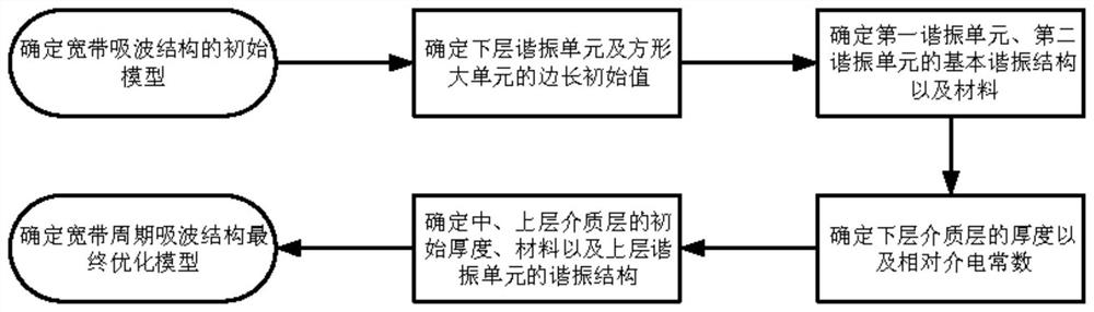
[0046] In order to better understand the design method proposed by the present invention, a large-angle broadband metamaterial wave-absorbing structure working in the Ku, K, and Ka bands is designed by applying the large-angle broadband metamaterial wave-absorbing structure design method proposed by the present invention below, The large-angle broadband metamaterial wave-absorbing structure proposed by the present invention is further described below in conjunction with the accompanying drawings and examples:

[0047] In this example, a large-angle broadband metamaterial absorbing structure needs to be designed. The center frequency of the working frequency band is 20 GHz. Therefore, the side length of the lower resonant unit ranges from 15 to 30 mm, and 23 mm is selected as the initial side length of the lower resonant unit.

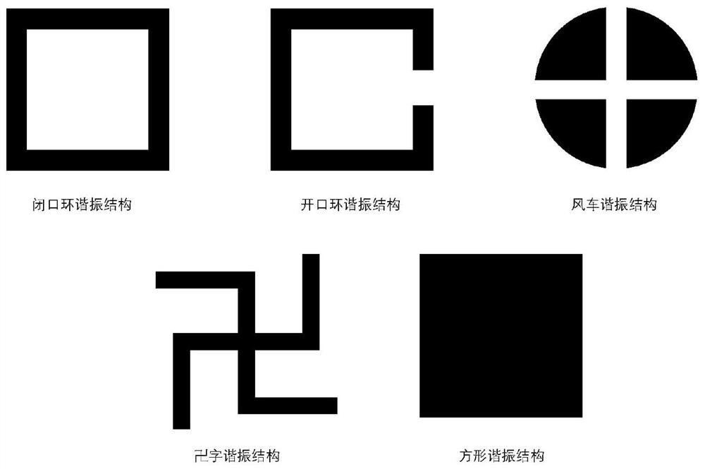
[0048] Considering the polarization insensitivity of the first and second resonant units and the broadband design requirements of the absorbing structur...


PUM


Abstract

The invention discloses a wide-angle broadband metamaterial wave-absorbing structure and a design method thereof, and belongs to the technical field of metamaterials. The wide-angle broadband metamaterial wave-absorbing structure is characterized by according to the near-field coupling theory of broadband metamaterial wave-absorbing structure design, considering a grating lobe effect and applying the destructive interference principle to obtain a periodic metamaterial wave-absorbing unit structure; arranging the first resonance units and the second resonance units in the same row in a staggered manner, and arranging the first resonance units and the second resonance units in two adjacent rows in a staggered manner for a half period so as to realize the large-angle incidence stability of the wave-absorbing structure on the basis of widening the absorption bandwidth; adjusting the structural size parameters of the periodic units and the thickness of a dielectric layer to adjust the absorption frequency corresponding to the wave-absorbing structure, and widening the wave-absorbing structure in a frequency band with the absorption rate of 70% or above through the mutual coupling of the resonance units of different structures. The metamaterial wave-absorbing structure designed by the invention is simple to prepare, is lower in processing technology requirement and is beneficial to batch production.

Description

technical field [0001] The invention belongs to the technical field of metamaterials, and in particular relates to a large-angle broadband metamaterial wave-absorbing structure and a design method thereof. Background technique [0002] The wave-absorbing structure was first used in the military field to reduce the radar cross section of flying weapon systems and improve the offensiveness and safety of flying weapons. With the in-depth study of absorbing structures, the application scenarios of absorbing structures have been broadened to more fields, such as: electromagnetic cloaks that realize the "stealth" function; radiation sensors that can detect visible light, infrared, laser or microwave radiation energy ; and ferrite absorbing structural ceramic tiles that improve the living environment of high-rise buildings. These applications all show that the absorbing structure has rich application scenarios and good development prospects in both the military field and the natio...

Claims


Application Information

Patent Timeline
Patent Type & Authority Applications(China)
IPC IPC(8): H01Q15/00H01Q17/00
CPCH01Q15/0026H01Q15/0086H01Q17/00
Inventor 吴泽威黄帅王敏行李泉立蒲友雷王建勋罗勇
Owner UNIV OF ELECTRONICS SCI & TECH OF CHINA
Why Eureka
Try Eureka