Linear voltage regulator circuit

A linear regulator and circuit technology, applied in instruments, regulating electrical variables, control/regulating systems, etc., can solve problems such as increasing the area of ​​the linear regulator circuit chip

Active Publication Date: 2021-12-03
PUYA SEMICON SHANGHAI CO LTD
View PDF8 Cites 0 Cited by
  • Summary
  • Abstract
  • Description
  • Claims
  • Application Information

AI Technical Summary

Problems solved by technology

Generally, the output voltage VDD needs to have driving capability. According to the required current flow, the width-to-length ratio of the driving MOS transistor Pm0 is usually taken as: Neglecting the effect of channel modulation, where β=μ*C ox , W is the channel width of the driving MOS transistor Pm0, L is the channel length of the driving MOS transistor Pm0, Ids is the source-drain current of the driving MOS transistor Pm0, Vgs_pm0 is the gate-source voltage of the driving PMOS transistor Pm0, Vth is the driving MOS transistor Pm0 Threshold voltage, μ is the carrier mobility, C ox is the capacitance of the

Method used


Image

  • Linear voltage regulator circuit
  • Linear voltage regulator circuit
  • Linear voltage regulator circuit

Examples


Embodiment 1

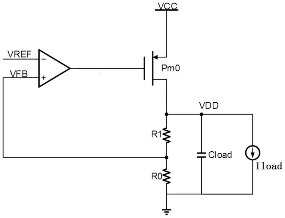
[0042] like figure 2 As shown, the linear voltage regulator circuit includes an operational amplifier AMP, a driving PMOS transistor Pm0, a zeroth voltage dividing resistor R0, a first voltage dividing resistor R1, a switch PMOS transistor Psw, a first current source I1, and a second current source I2;

[0043] The drive PMOS transistor Pm0 has its source terminal connected to the input voltage VCC, its drain terminal connected to the ground through the zero voltage dividing resistor R0 and the first voltage dividing resistor R1 connected in series, and its drain terminal is used as the output voltage VDD of the linear voltage regulator circuit output terminal;

[0044] The source end and the drain end of the switch PMOS transistor Psw are respectively connected to the output end of the operational amplifier AMP and the gate end of the driving PMOS transistor Pm0, and the gate end is grounded;

[0045] The negative input terminal of the operational amplifier AMP is connected...

Embodiment 2

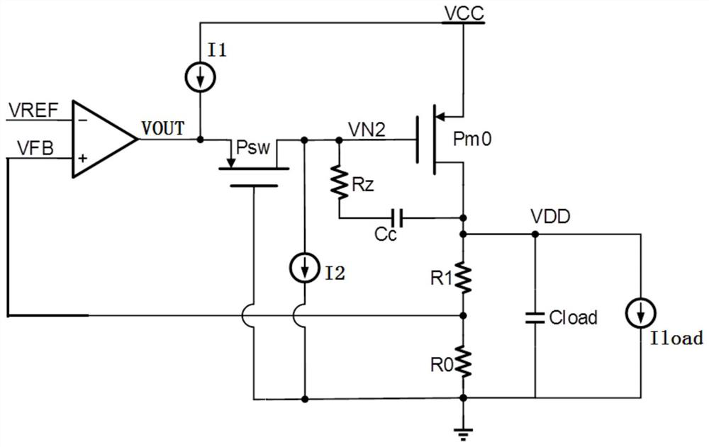
[0052] Based on implementation one, the linear voltage regulator circuit further includes a loop compensation resistor Rz and a loop compensation capacitor Cc;

[0053] The loop compensation resistor Rz and the loop compensation capacitor Cc are connected in series between the gate and drain of the driving PMOS transistor Pm0.

[0054] Preferably, the loop compensation resistor Rz is 100kΩ-200kΩ;

[0055] The loop compensation capacitor Cc is 1PF-10PF.

[0056] Preferably, the reference voltage VREF is provided by a bandgap reference (Bandgap voltage reference) circuit.

[0057] Preferably, a load capacitor Cload is connected between the drain terminal of the driving PMOS transistor Pm0 and the ground.

Embodiment 3

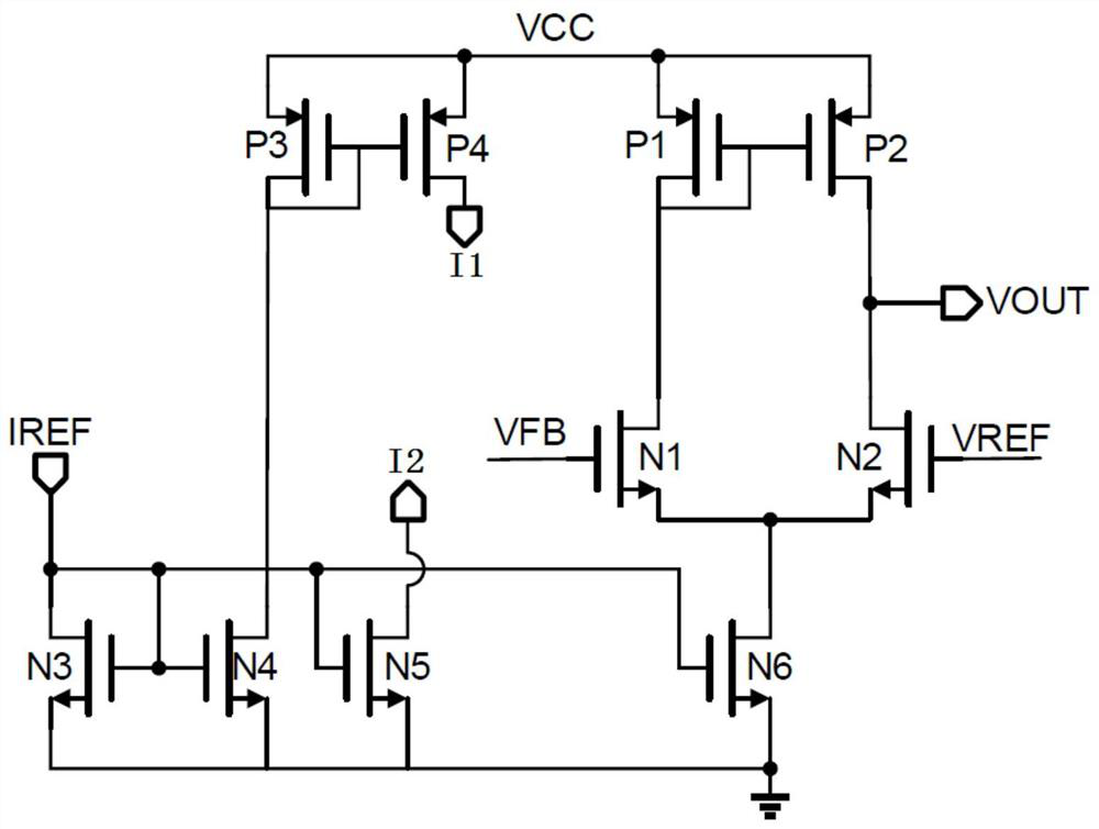
[0059] Based on the implementation of a linear regulator circuit such as image 3 As shown, the operational amplifier AMP, the first current source I1 and the second current source I2 form an operational amplifier circuit;

[0060] The operational amplifier circuit includes a first PMOS transistor P1, a second PMOS transistor P2, a third PMOS transistor P3, a fourth PMOS transistor P4, a first NMOS transistor N1, a second NMOS transistor N2, a third NMOS transistor N3, a fourth NMOS transistor N4, fifth NMOS transistor N5 and sixth NMOS transistor N6;

[0061] The gate terminal and the drain terminal of the first PMOS transistor P1 are short-circuited with the gate terminal of the second PMOS transistor P2;

[0062] The drain end of the first PMOS transistor P1 is connected to the drain end of the first NMOS transistor N1;

[0063] The drain end of the second PMOS transistor P2 is connected to the drain end of the second NMOS transistor N2, and serves as the output end of th...


PUM


Abstract

The invention discloses a linear voltage regulator circuit. A first current source, a second current source and a switch PMOS tube which are equal are added, the output of an operational amplifier provides gate-source voltage for the switch PMOS tube, the first current source and the second current source enable constant current to flow through the switch PMOS tube, and when the input voltage is lower and the linear voltage regulator circuit is heavily loaded, due to the fact that large current flows through the driving PMOS tube, the grid voltage of the driving PMOS tube is reduced, the switching PMOS tube is switched on, the output end of the operational amplifier is raised to the grid-source voltage of the switching PMOS tube, and meanwhile the grid voltage of the driving PMOS tube is not limited by the output of the operational amplifier, the output of the operational amplifier is not affected by the grid voltage of the driving PMOS tube under the low input voltage. The linear voltage regulator circuit can still output stable output voltage under the conditions of low input voltage and heavy load.

Description

technical field [0001] The invention relates to semiconductor circuit technology, in particular to a linear regulator circuit. Background technique [0002] Existing linear regulator circuits such as figure 1 As shown, it is composed of operational amplifier AMP, driving MOS transistor Pm0, zeroth voltage dividing resistor R0 and first voltage dividing resistor R1. [0003] The input voltage of this linear regulator is VCC, the output voltage is VDD, VREF is the reference voltage. Generally, the output voltage VDD needs to have driving capability. According to the required current flow, the width-to-length ratio of the driving MOS transistor Pm0 is usually taken as: Neglecting the effect of channel modulation, where β=μ*C ox , W is the channel width of the driving MOS transistor Pm0, L is the channel length of the driving MOS transistor Pm0, Ids is the source-drain current of the driving MOS transistor Pm0, Vgs_pm0 is the gate-source voltage of the driving PMOS transis...

Claims


Application Information

Patent Timeline
IPC IPC(8): G05F1/56
CPCG05F1/561
Inventor 周宁
Owner PUYA SEMICON SHANGHAI CO LTD
Why Eureka
Try Eureka